Chip-area reduction and congestion alleviation by timing-and-routability-driven empty-space propagation

a technology of empty space and chip area, applied in the direction of multi-objective optimization, cad techniques, instruments, etc., can solve the problems of unnecessary enlargement of the die size of the ic, inability to design the ic manually, and undesirable consequences

Inactive Publication Date: 2007-04-03
APEX DESIGN SYST
View PDF12 Cites 19 Cited by
  • Summary
  • Abstract
  • Description
  • Claims
  • Application Information

AI Technical Summary

Benefits of technology

[0015]In circuit design, after the cell placement process, empty-spaces are very often found among cells on a circuit layout. The process in accordance with the invention c

Problems solved by technology

As ICs become more complex, designing ICs manually no longer can be practical.
However, the most undesirable consequence of all is the unnecessary enlargement of the die size of the IC.
An IC with a larger die size is not only more expensive to manufacture in terms of material costs but also more susceptible to random defects during fabrication, thereby resulting in lower production yield.
On the other hand, too aggressive in the pursuit of die-size reduction may render the IC after placement ultimately unroutable.
However, the estimation is gross at best and very often is far off from the reality.
As such, some placed cells in the resultant layou

Method used


Image

  • Chip-area reduction and congestion alleviation by timing-and-routability-driven empty-space propagation
  • Chip-area reduction and congestion alleviation by timing-and-routability-driven empty-space propagation
  • Chip-area reduction and congestion alleviation by timing-and-routability-driven empty-space propagation

Examples


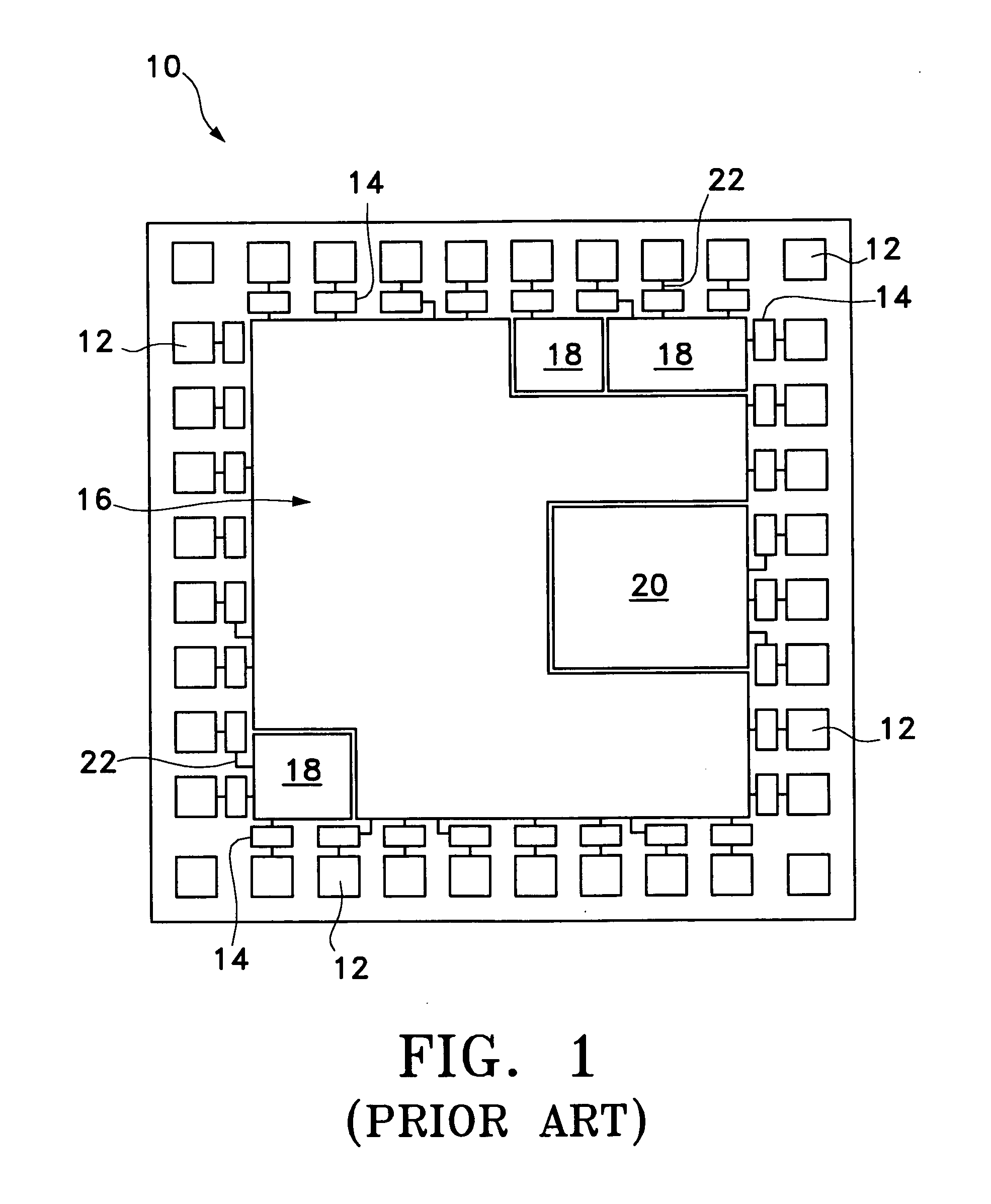
Embodiment Construction

[0035]The following description is presented to enable any person skilled in the art to make and use the invention. Details are set forth in the following descriptions for purpose of explanation. It should be appreciated that one of ordinary skill in the art would realize that the invention may be practiced without the use of these specific details. In other instances, well-known structures and processes are shown in block diagram forms in order not to obscure the description of the invention with unnecessary details. Thus, the present invention is not intended to be limited to be the embodiments shown, but is to be accorded with the widest scope consistent with the principles and features disclosed herein.

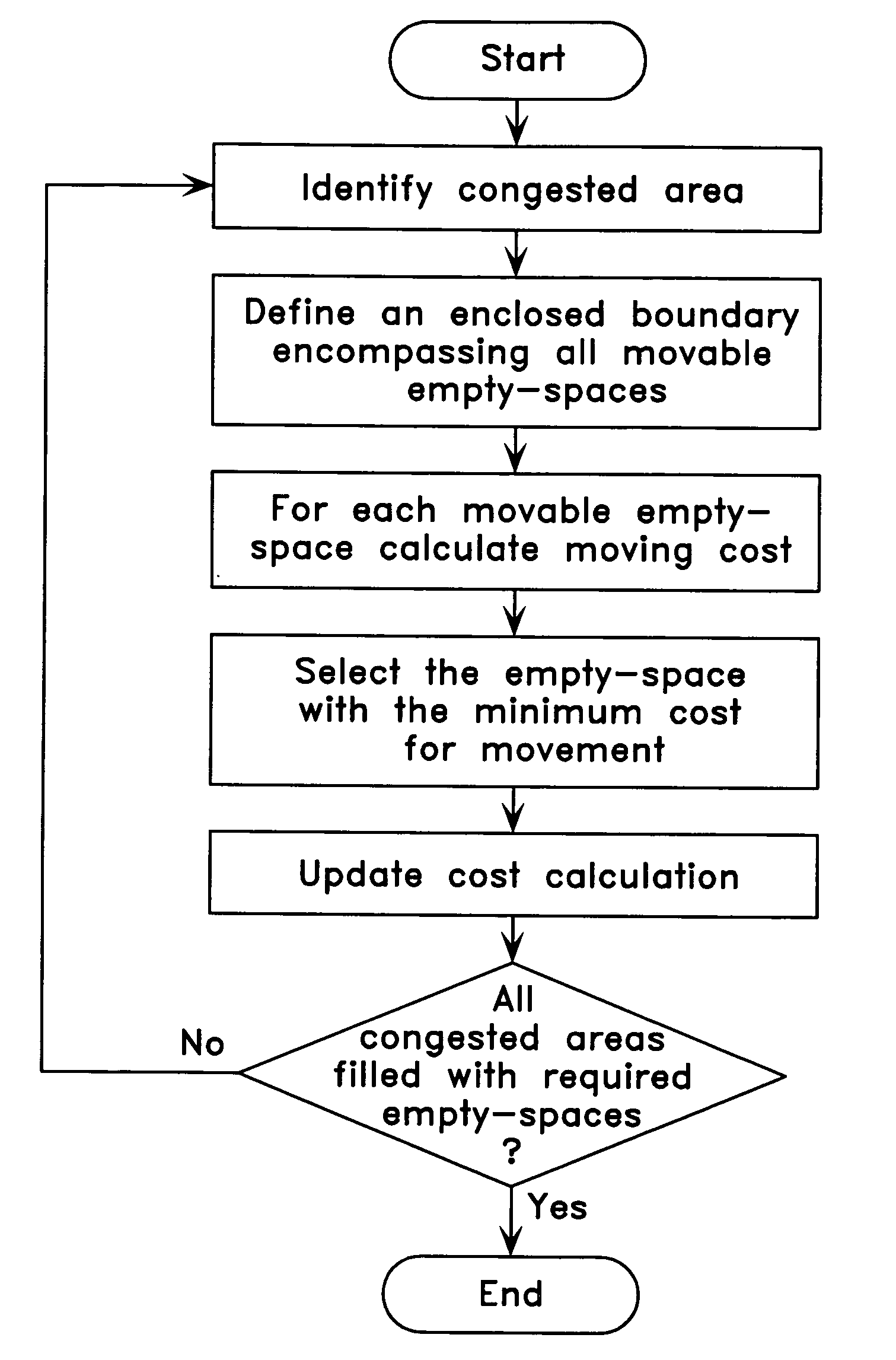
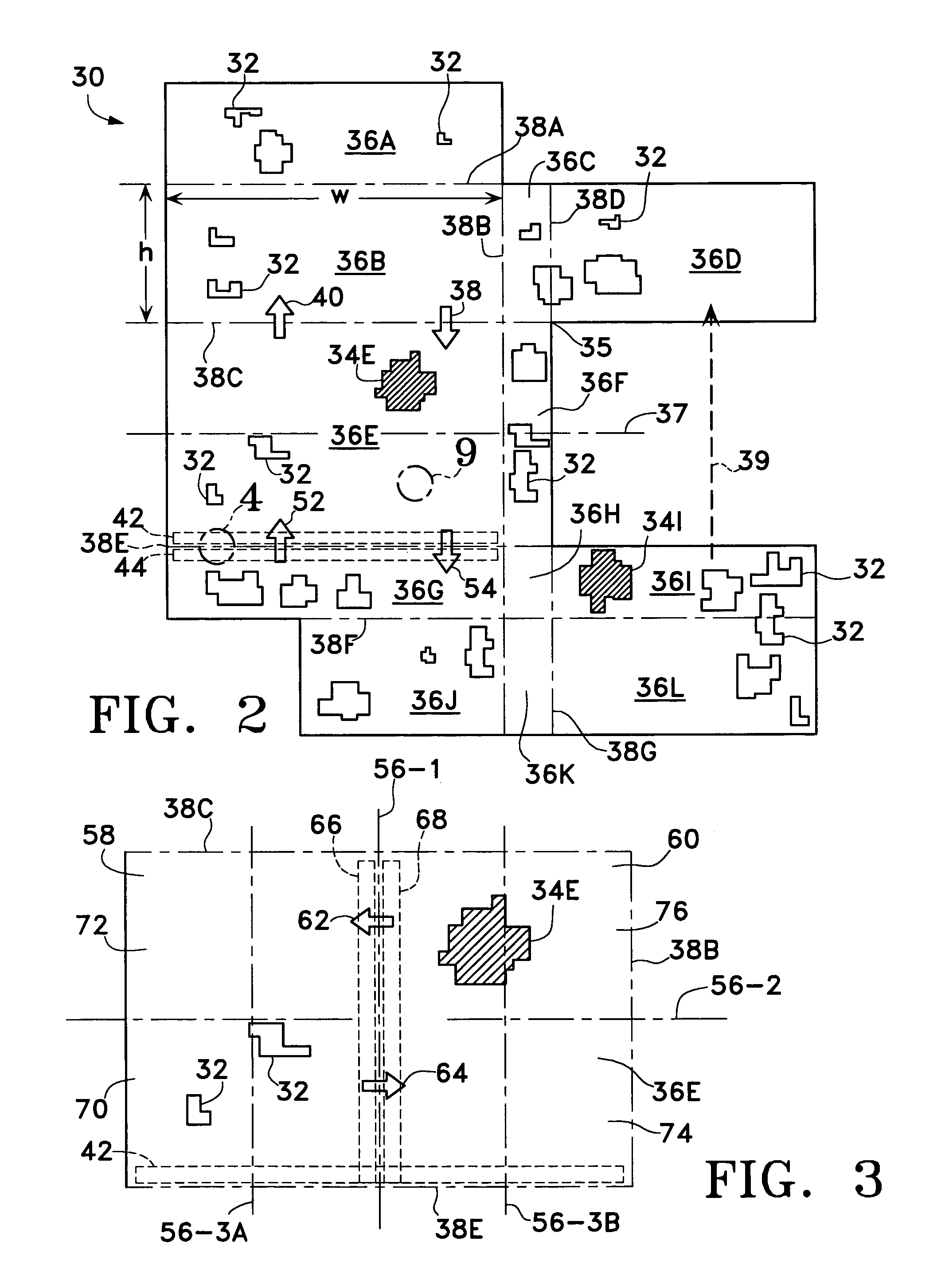
[0036]In the following description, the process of empty-space propagation of an IC layout is first described. Thereafter, application examples utilizing the inventive method for chip-size reduction and congestion alleviation are depicted.

Empty-Space Propagation

[0037]Empty-space p...


PUM


Abstract

An EDA (Electronic Design Automation) process which collects and moves empty-spaces among cells on a circuit layout to one or more target areas for productive use, such as chip-size reduction and routability congestion alleviation. The process includes globally moving the empty-spaces to the target area and thereafter locally moving the empty-spaces as refinement.

Description

CROSS-REFERENCE TO RELATED APPLICATIONS[0001]This application claims the benefit of an earlier filed U.S. Provisional Application No. 60 / 320,193, filed on May 14, 2003, the entirety of which is incorporated herein by reference.BACKGROUND OF THE INVENTION[0002]1. Field of the Invention[0003]The present invention generally relates to design of electronic circuits, and more particularly, to optimal placement and layout of circuit components in computer-aided design (CAD) of electronic circuits.[0004]2. Description of the Related Art[0005]The physical design of an integrated circuit (IC) includes placement of circuit components on the IC prior to fabrication. FIG. 1 is a simplified drawing of an exemplary IC floorplan signified by the reference numeral 10. The floorplan 10 corresponds to the die of the IC when fabricated. Disposed near the periphery of the floorplan 10 is a plurality of bonding pads 12. Adjacent to the bonding pads 12 is normally disposed a plurality of I / O (Input / Outpu...

Claims


Application Information

Patent Timeline
IPC IPC(8): G06F9/45G06F17/50
CPCG06F17/5072G06F2217/08G06F30/392G06F2111/06
Inventor KU, TSU-WEIFANG, WEN-CHUNG
Owner APEX DESIGN SYST
Why Eureka
Try Eureka