Method for forming, under a thin layer of a first material, portions of another material and/or empty areas

a technology of forming method and first material, applied in the direction of semiconductor/solid-state device manufacturing, electrical equipment, transistors, etc., can solve the problems of difficult control of the thickness of the buried layer, the inability to form a buried layer of any type of material, and the relatively destructive effect of the implantation technique on the upper part of the substra

Active Publication Date: 2007-04-10
STMICROELECTRONICS SRL +1
View PDF18 Cites 7 Cited by
  • Summary
  • Abstract
  • Description
  • Claims
  • Application Information

AI Technical Summary

Benefits of technology

[0010]Another object of the present invention is to provide such a method which is non-destructive for the layer of a given material.

Problems solved by technology

This implantation technique is however relatively destructive for the upper part of the substrate.
Further, it does not enable forming a buried layer of any type of material.
Further, the thickness of the buried layer is difficult to control.
Once the layer has been deposited, no known technique enables removing chosen portions of the dielectric or conductive layer.
A disadvantage of this technique thus is that the deposited layer necessarily has a shape identical to that of the silicon / germanium layer.

Method used


Image

  • Method for forming, under a thin layer of a first material, portions of another material and/or empty areas
  • Method for forming, under a thin layer of a first material, portions of another material and/or empty areas
  • Method for forming, under a thin layer of a first material, portions of another material and/or empty areas

Examples


Embodiment Construction

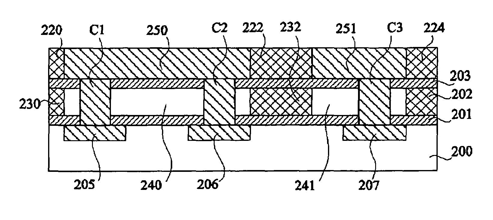
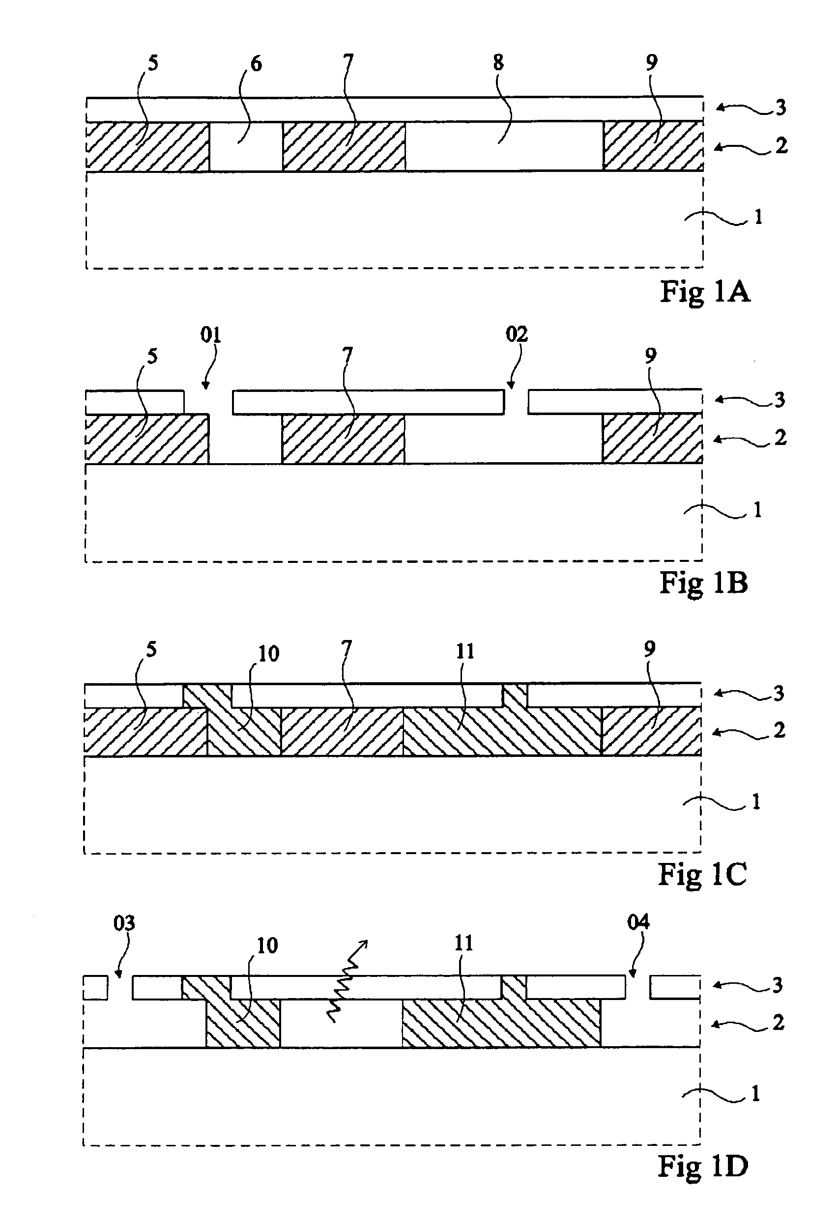
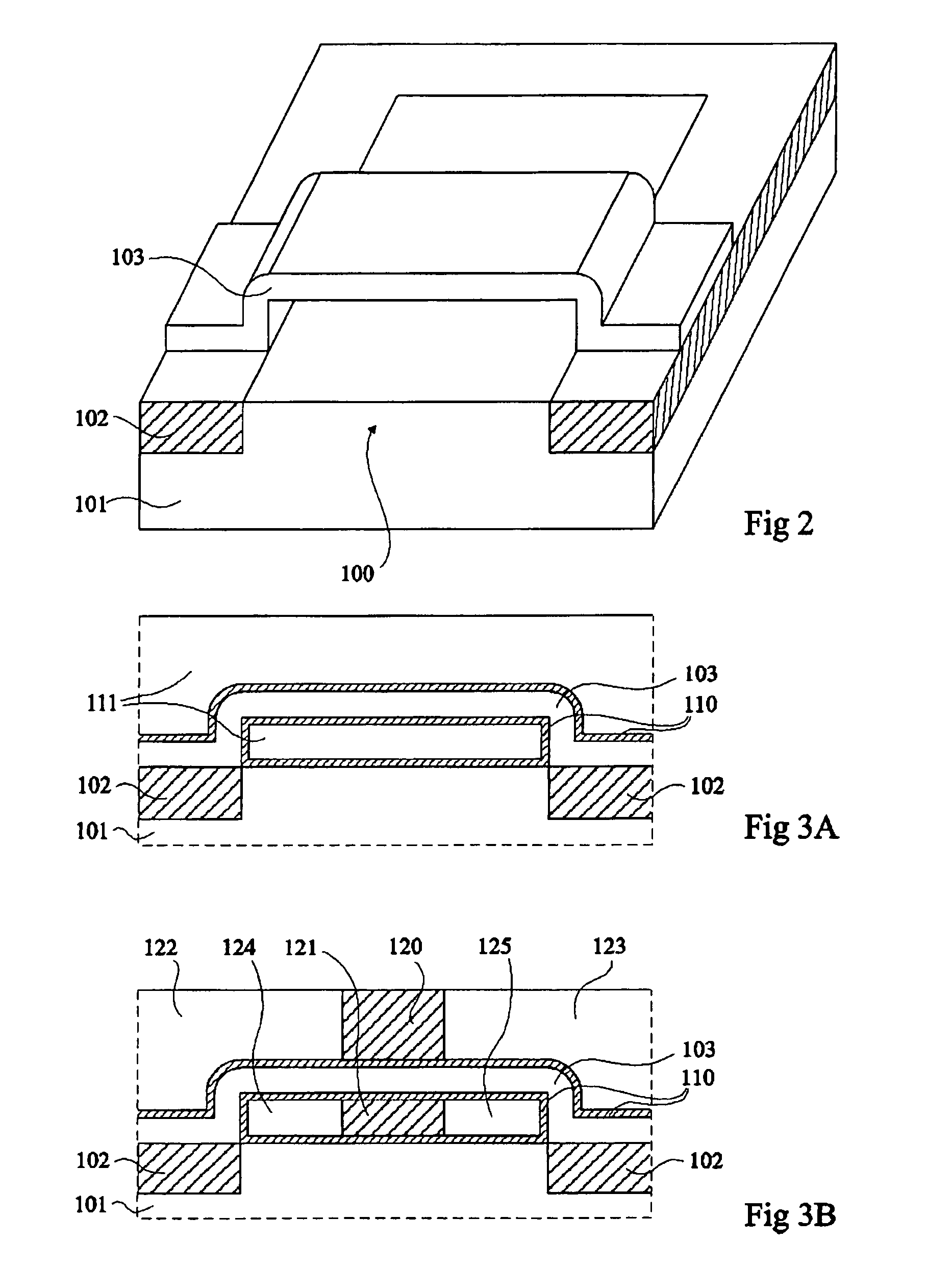
[0027]For clarity, the same elements have been designated with the same reference numerals in the different drawings and, further, as usual in the representation of integrated circuits, the drawings are not to scale.

[0028]The general aspects of the method of the present invention are described in relation with FIGS. 1A to 1D. Examples of implementation of the method are described hereafter for the forming of a transistor of SON type and for the forming of an interconnect network enabling connecting the components of a circuit to one another.

[0029]In an initial step, illustrated in FIG. 1A, a stacking of a photosensitive layer 2 and of a thin layer 3 of a given material is formed on a substrate 1. Substrate 1 may have any structure obtained after a step of a standard integrated circuit forming method. The stacking of photosensitive layer 2 and of thin layer 3 may be obtained according to various methods as will appear in the examples of implementation of the method of the present inv...


PUM

PropertyMeasurementUnit
thicknessaaaaaaaaaa
photosensitiveaaaaaaaaaa
conductiveaaaaaaaaaa

Abstract

A method for forming a empty area under a layer of a given material, including forming on a substrate a stacking of a photosensitive layer and of a layer of the given material; insolating a portion of the photosensitive layer or its complement according to whether the photosensitive layer is positive or negative with an electron beam crossing the layer of the given material; and removing the portion of the photosensitive layer.

Description

BACKGROUND OF THE INVENTION[0001]1. Field of the Invention[0002]The present invention relates to integrated circuit manufacturing methods.[0003]The method of the present invention more specifically aims at forming, under a layer of a first material, empty areas and / or portions of another material.[0004]2. Discussion of the Related Art[0005]Known ion implantation techniques enable forming buried layers in a substrate by having implanted ions react with the substrate. An example of an ion implantation is the implantation of oxygen O2 in a silicon substrate to form buried silicon oxide layers SiO2.[0006]This implantation technique is however relatively destructive for the upper part of the substrate. Further, it does not enable forming a buried layer of any type of material. Further, the thickness of the buried layer is difficult to control.[0007]Another known buried layer forming technique is that implemented for example upon forming of devices of SON (silicon on nothing) type. After ...

Claims


Application Information

Patent Timeline
Patent Type & Authority Patents(United States)
IPC IPC(8): H01L21/4763G03F7/11G03F7/20G03F7/36G03F7/40H01L21/027H01L21/3205H01L21/336H01L21/768H01L27/12H01L29/423H01L29/786
CPCH01L21/0277H01L21/7682H01L29/42384H01L29/42392H01L29/66772H01L29/78654
Inventor CORONEL, PHILIPPELAPLANCHE, YVESPAIN, LAURENT
Owner STMICROELECTRONICS SRL
Why Eureka
Try Eureka