Solid-state image pickup exposure control system and method

Inactive Publication Date: 2007-04-10
SONY CORP
View PDF9 Cites 6 Cited by
  • Summary
  • Abstract
  • Description
  • Claims
  • Application Information

AI Technical Summary

Benefits of technology

[0015]The present invention has been developed in view of the above problem. It is an object of the present invention to provide a solid-state image pickup device which accurately detects th

Problems solved by technology

Although the motion of the object is detected, the image of the object looks doubled, and it is difficult to correctly recognize the image.
However, this is not the case If

Method used


Image

  • Solid-state image pickup exposure control system and method
  • Solid-state image pickup exposure control system and method
  • Solid-state image pickup exposure control system and method

Examples


first embodiment

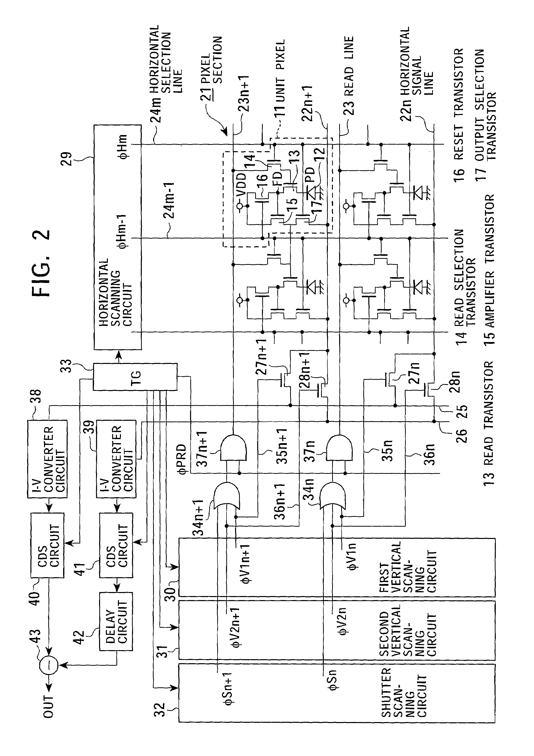
[0037]FIG. 2 is a block diagram illustrating the CMOS imager in accordance with the Referring to FIG. 2, a unit pixel 11 is represented by an area surrounded by a broken line. The unit pixel 11 includes five N-channel MOS transistors of a read transistor 13, a read selection transistor 14, an amplifier transistor 15, a reset transistor 16, and an output selection transistor 17 with respect to a photodiode (PD) 12 as a photoelectric conversion element. The unit pixels 11 are arranged in a matrix form, thereby forming a pixel section 21.

[0038]For simplification of FIG. 2, the pixel section 21 includes pixels of two columns ((m−1)-th and m-th) and two rows (n-th and (n+1)-th). Arranged in the pixel section 21 are horizontal signal lines 22n+1 and 22n and read lines 23n+1 and 23n. Further arranged are horizontal selection lines 24m−1 and 24m.

[0039]The construction of the unit pixel 11 at m-th column and (n+1)-th row is specifically discussed. In the unit pixel 11, the photodiode 12 pe...

second embodiment

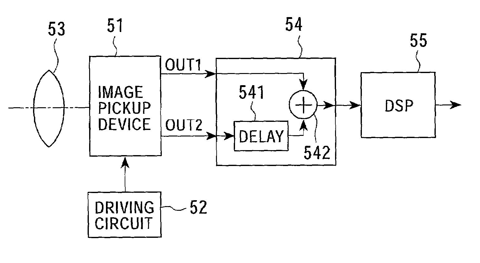
[0088]the present invention is discussed in detail below with reference to the drawings, wherein the present invention is applied to an X-Y addressing type solid-state image pickup device such as a CMOS imager.

[0089]FIG. 13 is a block diagram of a CMOS imager in accordance with the second embodiment of the present invention. With reference to FIG. 13, the second embodiment remains unchanged from the first embodiment except that the second embodiment employs an adder 143 instead of the subtracter 43 in the first embodiment, and the general discussion of the second embodiment is omitted.

[0090]A variety of signal processing circuits such as an AGC (automatic gain control) circuit or an ADC (analog digital converter) circuit may be added as a stage subsequent to the adder 143.

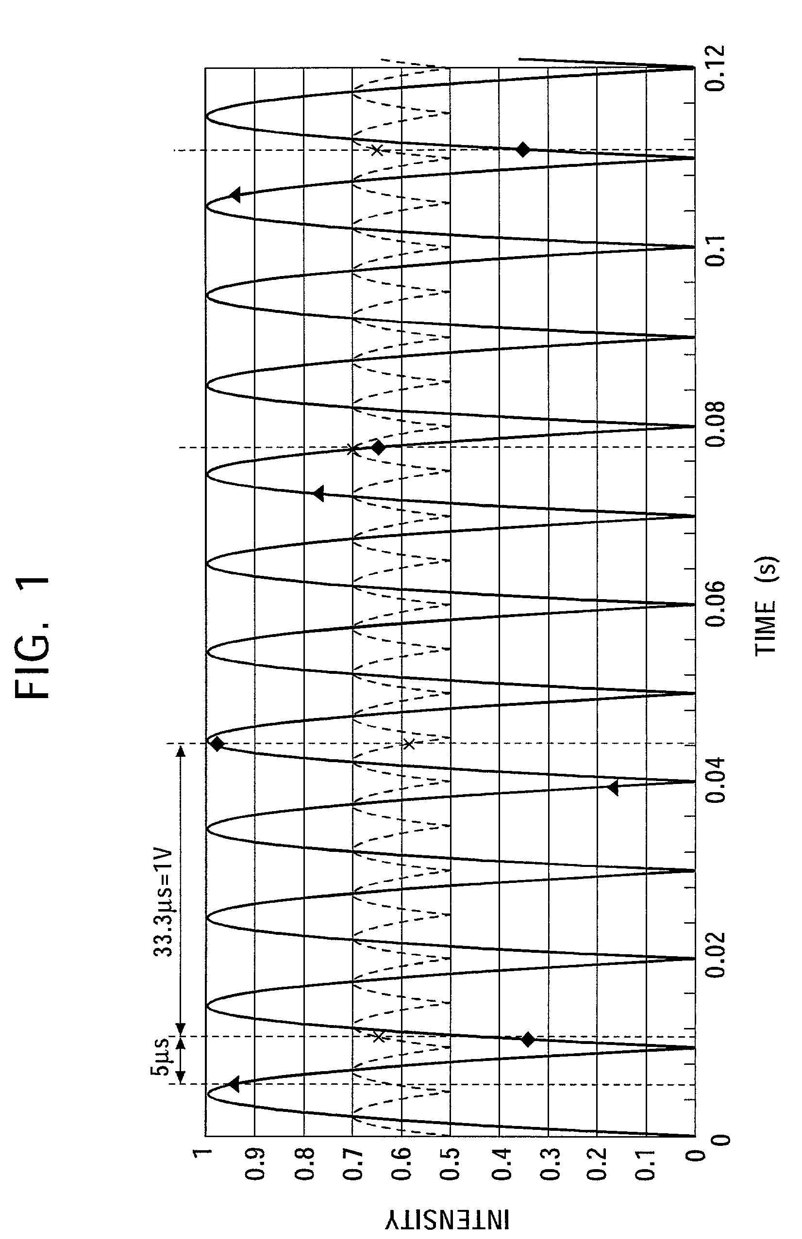
[0091]When the frequency of the AC utility power in the area where the CMOS imager is used is A [Hz], the first and second vertical scanning circuits 30 and 31 successively output two vertical scanning pulses φVn1 ...


PUM


Abstract

If image data of a prior frame and image data of a current frame are compared with each other, a resulting image appears doubled because the distance of travel of an object within one frame becomes long when the object moves quickly.
In a focal-plane shutter type CMOS imager which performs exposure row by row, a shutter scanning circuit 32 performs exposure twice with exposure time divided into two durations on one pixel 11 in a pixel section 21. Signals based on the two exposure durations from the one pixel are read through respective vertical signal lines 25 and 26 under the control of vertical scanning circuits 30 and 31. The two signals are then synchronized through the delay circuit 42, and a difference between the two signals is determined through the subtracter 43, and the difference signal is output. The motion of an object is detected based on the difference signal.

Description

[0001]This application claims priority to Japanese Patent Application Nos. JP2001-210269 and JP2001-210268 each of which were filed on Jul. 11, 2001 and which are herein incorporated herein by reference.BACKGROUND OF THE INVENTION[0002]1. Field of the Invention[0003]The present invention relates to a solid-state image pickup device, a method for driving the solid-state image pickup device, a motion detector, and a camera system and, more particularly to a solid-state image pickup device which successively reads a pixel signal from a pixel section, a method for driving the solid-state image pickup device, a motion detector that uses the solid-state image pickup device as an imaging device, and a camera system.[0004]2. Description of the Related Art[0005]The solid-state image pickup devices are mainly divided into a charge-transfer solid-state image pickup device such as a CCD imaging sensor and an X-Y addressing type solid-state image pickup device such as a CMOS imager. These two ty...

Claims


Application Information

Patent Timeline
IPC IPC(8): H04N5/335H04N7/18H04N5/14H04N5/353H04N5/357H04N5/374H04N5/376
CPCH04N3/155H04N5/2329H04N5/335H04N5/144H04N23/689H04N25/53H04N25/531H04N25/00
Inventor SUZUKI, RYOJI
Owner SONY CORP
Why Eureka
Try Eureka