Word line driving circuit with a word line detection circuit

a detection circuit and driving circuit technology, applied in the field of semiconductor storage devices, can solve the problems of increasing block size, complicating circuitry, and controlling signals generated by timing generators provided at a specified location that cannot cope with skew distortion, and achieve the effect of simplifying circuit configuration and stable operation

Active Publication Date: 2007-04-10
LONGITUDE LICENSING LTD
View PDF9 Cites 1 Cited by
  • Summary
  • Abstract
  • Description
  • Claims
  • Application Information

AI Technical Summary

Benefits of technology

[0006]In a test mode, frequently used in a DRAM test, it may be an occurrence that the word line is activated during the time duration several to tens of times longer than in a normal operation. In such case, the word line decay time (fall time) becomes longer than usual, so that the switching of the pull-down timing from GND to VBB needs to be carried out by a control operation consistent with the time duration of activation. The result is that plural delay elements need to be provided in the timing generator and switched depending on the operating mode, thus complicating the circuitry.
[0022]According to the present invention, control is exercised so that, during the rise or fall of the word line driving signal, the signal level of the word line driving signal is fed back in the driving control circuit, and the changes in the signal level of the word line driving signal per se are detected to effect a two-stage operation. Hence, there is no necessity of providing external control circuits or external delay elements for achieving the two-stage operation, thus simplifying the circuit configuration. No timing adjustment is needed for carrying out the two-stage operation, thus assuring stable operations.

Problems solved by technology

A plural number of the signal generating circuits are sporadically distributed within the DRAM chip, such that, a control signal generated by the timing generator provided at a specified location cannot cope with the skew distortion which depends on the layout-based location of the circuit.
Consequently, for managing timing control within the signal generating circuit, it is necessary to provide a delay device for each circuit, thus necessarily increasing the block size.
The result is that plural delay elements need to be provided in the timing generator and switched depending on the operating mode, thus complicating the circuitry.
Moreover, should there be level variations in the power supply VDD, the delay time in the delay elements is varied, so that the voltage pull-down start timing cannot be controlled in stability.

Method used


Image

  • Word line driving circuit with a word line detection circuit
  • Word line driving circuit with a word line detection circuit
  • Word line driving circuit with a word line detection circuit

Examples


first embodiment

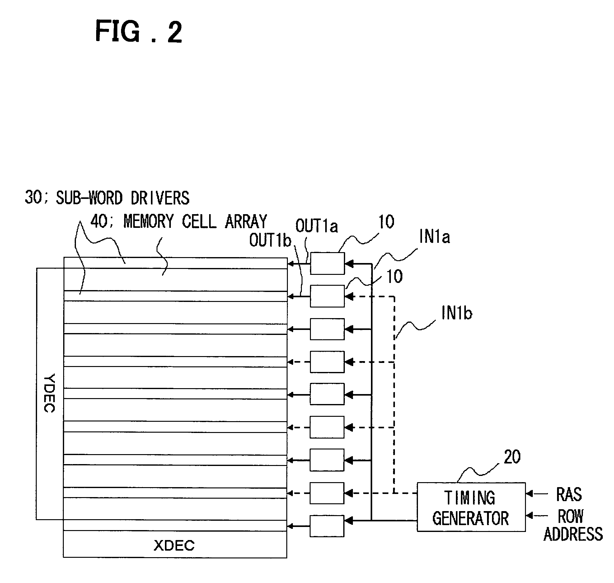
[0031]Next, typical circuits, embodying the present invention, are explained in detail. FIG. 2 depicts a block circuit diagram showing a word line driving circuit of a DRAM as a main component of the present invention. The chip of the DRAM in its entirety is split in eight parts for forming plural memory blocks or banks. These blocks, resulting from division into eight parts, include a memory cell array 40 of a similar structure, respectively. On both sides of each memory cell array 40 are arranged sub-word drivers 30. A Y decoder YDEC is provided for extending along one side (end) of the memory cell arrays 40, and an X decoder XDEC is arranged for extending at right angles to the Y decoder. A plurality of sub-word lines, not shown, extend vertically from the X decoder XDEC, whilst a plurality of Y-selecting lines, not shown, extend from the Y decoder YDEC. A memory cell is selected by one of the sub-word lines and one of the Y selecting lines for access.

[0032]In FIG. 2, a timing ge...

second embodiment

[0045]FIG. 5 depicts a circuit diagram showing a driving circuit of a word line of a semiconductor storage device according to a second embodiment of the present invention. The driving circuit of the second embodiment corresponds to the driving circuit of the first embodiment to which is included a circuit for enabling two-stage operation, even on startup. In FIG. 5, the same reference numerals as those of FIG. 3 denote the same or equivalent parts and the corresponding explanation is omitted. In FIG. 5, an FET Q16, a NOR circuit NOR1, a NOR circuit NOR2 and an inverter circuit INV6 are added to FIG. 3.

[0046]The source of the FET Q16 is connected to VDD, and the drain thereof is connected to the drain of the FET Q13, the drain of the FET Q14 and to the drain of the FET Q15 to generate an output signal OUT2 of the driving circuit. In addition, the drain of the FET 16 is connected to one input terminal of the NOR circuit NOR1. The drain of the FET Q16 is connected to an input terminal...


PUM


Abstract

A semiconductor storage device having a word line driving circuit of a small circuit scale, and operating in stability. The device includes a first driving circuit 11 for driving a word line driving signal 15 towards a first potential, a second driving circuit 12 for driving the word line driving signal 15 towards a second potential, a third driving circuit 13 for driving the word line driving signal 15 to a third potential, and a driving control circuit 14. This driving control circuit 14 actuates the first driving circuit 11 when the input signal 16 is at a first logical value, while actuating the second driving circuit 12 when the input signal 16 transfers from the first logical value to the second logical value and actuating the third driving circuit 13 on detection that the word line driving signal 15 has been driven towards the second potential.

Description

FIELD OF THE INVENTION[0001]This invention relates to a semiconductor storage device and, more particularly, to a semiconductor storage device including a driving circuit for a word line used for accessing a memory cell.BACKGROUND OF THE INVENTION[0002]A semiconductor storage device, including memory cells at the points of intersection of word lines and bit lines, arranged at right angles thereto, is finding widespread use in many fields of applications. With this semiconductor storage device, a negative word line system, in which the ‘floating’ of the VBB level of the negative potential at the time of resetting the word line is suppressed to diminish the leakage current of, e.g., the memory cell, has been known and disclosed in, e.g., Patent Publication 1. In the word line driving circuit of the Patent Document 1, the voltage on the word line is pulled down to the potential VSS (ground potential), after which the word line voltage is lowered to VBB (negative potential) that is lowe...

Claims


Application Information

Patent Timeline
Patent Type & Authority Patents(United States)
IPC IPC(8): G11C8/08G11C8/00G11C11/407
CPCG11C8/08
Inventor FUJIMA, SHIRO
Owner LONGITUDE LICENSING LTD
Why Eureka
Try Eureka