Line driver with reduced power consumption

a technology of power consumption and line driver, applied in the field of signal communication, can solve the problems of increasing the length of the line being charged or discharged, increasing the linear proportion of power consumption, and excessive radiated energy,

Active Publication Date: 2007-04-10
BENHOV GMBH LLC
View PDF12 Cites 5 Cited by
  • Summary
  • Abstract
  • Description
  • Claims
  • Application Information

AI Technical Summary

Benefits of technology

[0022]The present invention seeks to reduce the energy needed to drive a line by reducing the drive voltage or current after the state has changed providing means able to produce shorter pre-emphasized signals not determined by the clock.
[0024]The present invention is a means to reduce the power consumption of a chip by sending state changes through at full drive strength, then reducing the strength such that the line capacitance decays through the terminating resistors or discharge transistors, such that when the next state change is needed, then line has less stored energy needing to be discharged.
[0026]a means for reducing the power consumption of the transmitter, including:
[0039]In another aspect, the invention is a method of reducing the power consumption of a transmitter in a high speed communication system comprising a chip having a transmitter with a set of driving transistors for driving a signal representing transmitted data into a communication line connecting the transmitter and a receiver,
[0048]In still another aspect, a means for reducing power consumption in a high speed communication system comprising a chip having a transmitter with a set of driving transistors for driving a signal representing transmitted data into a communication line connecting the transmitter and a receiver,

Problems solved by technology

In this case, the length of the line being charged or discharged is increased, compared to sending a pure clock signal, and this again increases the power consumption in linear proportion to the ratio of the frequency of bit interval changes to the clock frequency.
Another factor in very high speed systems is that the driver must be differential: without this the currents injected into the power supplies and the radiated energy becomes excessive.
The power supply noise created on switching is a critical factor in these systems.
The predriver can often consume more power than the driver when there is a heavily capacitive load due to the reflected Miller capacitance.
However, power savings obtained by using the method and circuitry of Jong et al. are insufficient.
This may be tolerable at relatively low-speeds; however, high-speed communications can require shorter pre-emphasized signals.
In the above context, long pre-emphasized signals do not match high-speed communications and obviously lead to excessive power consumption.

Method used


Image

  • Line driver with reduced power consumption
  • Line driver with reduced power consumption
  • Line driver with reduced power consumption

Examples


Embodiment Construction

[0057]A detailed description of the present invention will now be given, without loss of generality, and with reference to the following figures:

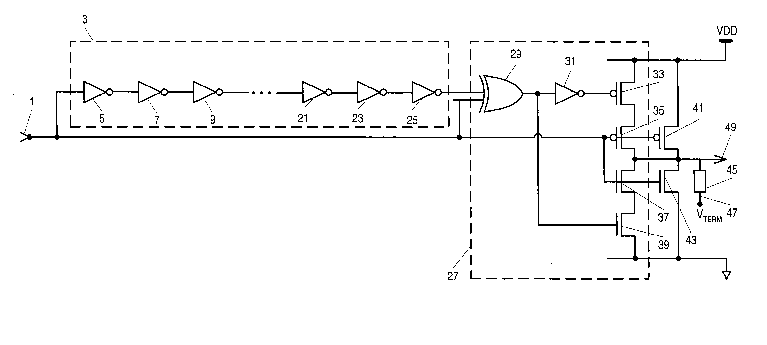
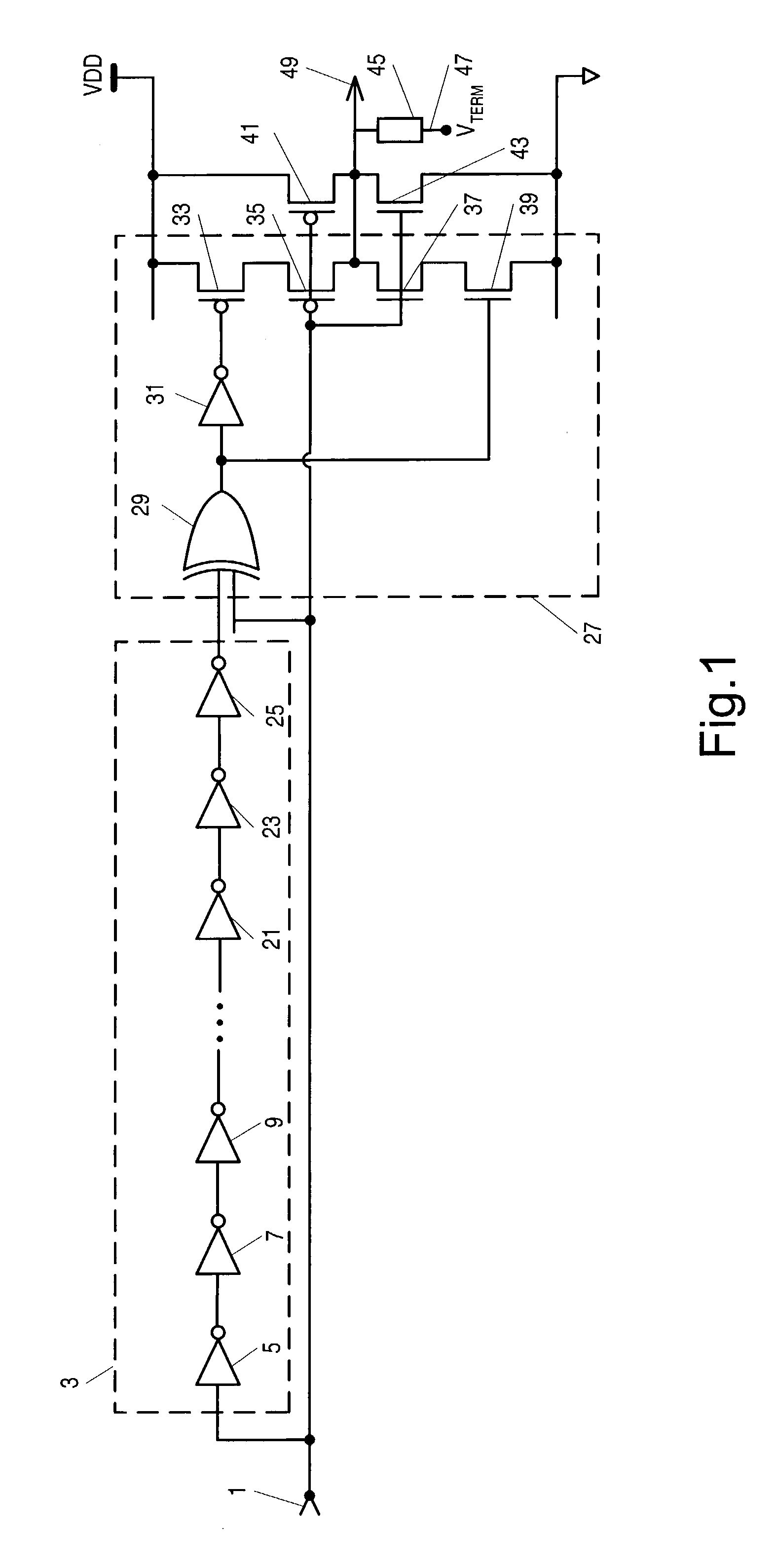
[0058]A block diagram in FIG. 1 shows an embodiment of the present invention in which an input signal 1 drives a transmitter comprising a strong transistor set 33, 35, 37 and 39 for driving a signal at a high slew rate, i.e. at a slew rate sufficient to change the transmission line state in required time interval, and a weak transistor set 41 and 43 for maintaining the transmission line state at a level sufficient to maintain the state of a receiver at the other end of the transmission line. The output line is terminated to a terminating voltage Vt by a resistance 45.

[0059]The strong transistor set is driven for a short interval such as by a delayed instance of the input signal 1 using a delay chain 3 comprising a series of inverters 5, 7, 9 to 21, 23, 25. The delay chain 3 stores the recent history of the transmission line, i.e. the state ...


PUM


Abstract

A means for reducing the power consumption of the transmitter by storing the recent history of the transmitted data using a string of gates with taps from the string taken at points determined by the propagation delay of each gate and controlling driving transistors as a function of comparison of that history with input data so that, either the signal is driven into the transmission line at full strength, or at a level near the minimum needed to retain the state in the receiver.The advantage of the invention is that the line capacitance decays through the terminating resistors or discharge transistors, such that when the next state change is needed, then line has less stored energy needing to be discharged.

Description

BACKGROUND OF THE INVENTION[0001]1. Technical Field[0002]The present invention relates to the communication of signals, in particular, to the transmission and reception of digital signals, where the signals are at a very high frequency.[0003]The present invention is particularly applicable to interfaces between integrated circuits and for high speed communications, such as currently addressed by Asynchronous Transfer Mode (ATM), Gigabit Ethernet, SONET, 3GIO, RapidIO, Hyperchannel and Fibre Transmission Channels.[0004]2. Background of the Invention[0005]The input buffers to an integrated circuit comprise a series of open loop amplifiers, commonly of an inverting type (inverters). This means that the input signal need only switch a few millivolts around a voltage threshold, plus a noise margin, for the signal to switch logic states, the minimum Vil and Vih levels.[0006]Transmission lines between integrated circuits are predominantly capacitive in their characteristic at very high fre...

Claims


Application Information

Patent Timeline
Patent Type & Authority Patents(United States)
IPC IPC(8): H04B3/00H04L25/00H04L25/02
CPCH04L25/028H04L25/0272H04L25/0292
Inventor DEAS, ALEXANDER ROGERABROSIMOV, IGOR ANATOLIEVICH
Owner BENHOV GMBH LLC
Why Eureka
Try Eureka