Semiconductor device and method of producing the same

a semiconductor and semiconductor technology, applied in the direction of semiconductor/solid-state device manufacturing, semiconductor devices, semiconductor devices, etc., can solve the problems of difficult to reduce the collector resistance at the bottom portion, and achieve the effect of reducing the collector resistance of the bipolar transistor

Inactive Publication Date: 2007-04-17
LAPIS SEMICON CO LTD
View PDF4 Cites 17 Cited by
  • Summary
  • Abstract
  • Description
  • Claims
  • Application Information

AI Technical Summary

Benefits of technology

[0015]In the method of producing the semiconductor, in particular the bipolar transistor, the second oxide layer is removed to form the cavity, and the polycrystalline silicon layer is formed in the cavity. Accordingly, it is possible to form the polycrystalline silicon layer with an appropriate shape at a bottom portion of the second single crystal layer in the bipolar transistor forming area. With the polycrystalline silicon layer, it is possible to reduce a collector resistance of the bipolar transistor.

Problems solved by technology

When the bipolar transistors are mounted in a single chip together with MOSFETs capable of high density mounting, it is possible to obtain performance difficult to achieve in an LSI formed only of MOSFETs.
However, when a vertical type bipolar transistor with high performance and high mounting density is produced, it is still difficult to reduce a collector resistance at a bottom portion thereof.

Method used


Image

  • Semiconductor device and method of producing the same
  • Semiconductor device and method of producing the same
  • Semiconductor device and method of producing the same

Examples


Embodiment Construction

[0023]Hereunder, embodiments of the present invention will be explained with reference to the accompanying drawings. A configuration and arrangement of an embodiment are schematically presented for explaining the invention. The embodiments will be explained with configurations (materials) and numerical conditions as preferred examples, and the invention is not limited thereto.

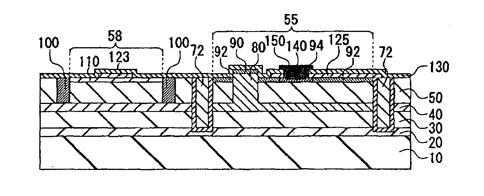
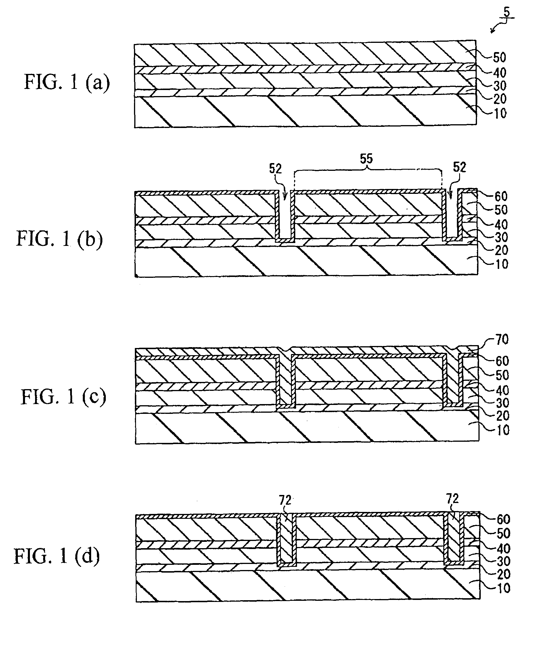
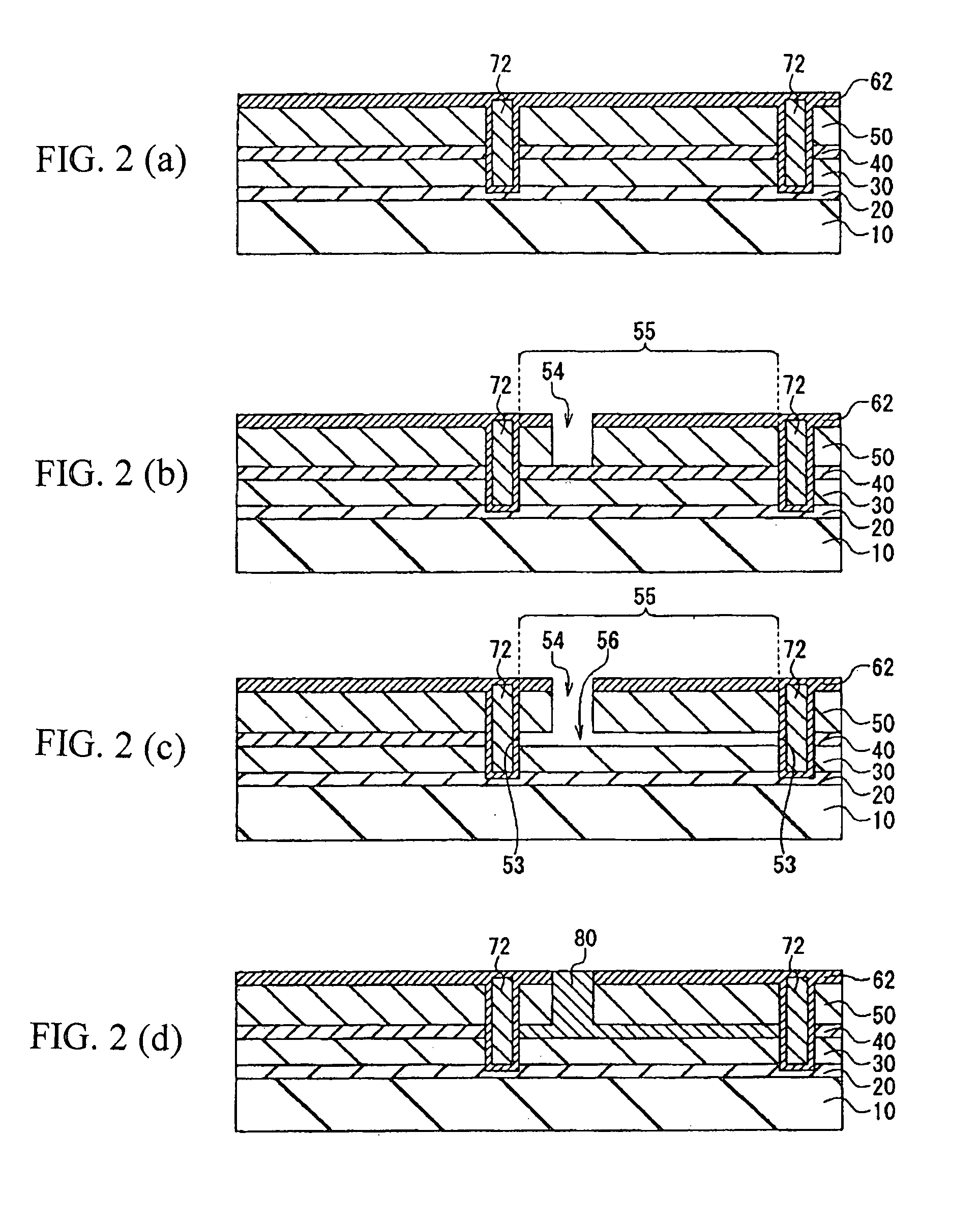
[0024]FIGS. 1(A) to 1(D) to 6(A) to 6(C) are views showing a process of producing a BiCMOS having a bipolar transistor and a CMOS both formed on a same single substrate as semiconductor devices. First, a double SOI substrate 5 having a double SOI structure is prepared. The double SOI substrate 5 has a laminated structure in which, on a semiconductor substrate 10 such as a silicon substrate, a first oxide layer 20, a first single crystal silicon layer 30, a second oxide layer 40, and a second single crystal silicon layer 50 are formed sequentially in this order. When the double SOI substrate 5 is prepared, a sil...


PUM

PropertyMeasurementUnit
thicknessaaaaaaaaaa
thicknessaaaaaaaaaa
thicknessaaaaaaaaaa

Abstract

A method of producing a semiconductor device includes the steps of: preparing a double SOI substrate, forming a deep trench, filling the deep trench, forming an opening, forming a cavity, depositing a polycrystalline silicon layer, and forming a bipolar transistor.

Description

BACKGROUND OF THE INVENTION AND RELATED ART STATEMENT[0001]The present invention relates to a semiconductor device and a method of producing the semiconductor device.[0002]A bipolar transistor is capable of running at a high speed as compared with a MOSFET, and has a high current drive performance. Therefore, the bipolar transistor is suitable for an LSI for driving a laser for light transmission or a power amplifier of a cellular phone. When the bipolar transistors are mounted in a single chip together with MOSFETs capable of high density mounting, it is possible to obtain performance difficult to achieve in an LSI formed only of MOSFETs.[0003]A conventional process of producing a BiCMOS formed of bipolar transistors and CMOSs, i.e., p-type MSFETs and n-type MOSFETs, on a single chip will be explained with reference to FIGS. 7(A) to 7(C) (refer to Patent Reference 1). FIGS. 7(A) to 7(C) are views showing a conventional process of producing the BiCMOS.[0004]A silicon oxide layer 220...

Claims


Application Information

Patent Timeline
Patent Type & Authority Patents(United States)
IPC IPC(8): H01L31/00H01L21/8222
CPCH01L21/84H01L27/1203H01L29/66265H01L29/7317
Inventor FUJIMAKI, HIROKAZU
Owner LAPIS SEMICON CO LTD
Why Eureka
Try Eureka