Semiconductor device

a technology of semiconductor devices and devices, applied in semiconductor devices, semiconductor/solid-state device details, electrical apparatus, etc., can solve problems such as adverse effects, long line lengths, signal delay, and increased noise, and achieve the effect of effectively solving problems

Inactive Publication Date: 2007-04-17
MAXELL HLDG LTD
View PDF21 Cites 1 Cited by
  • Summary
  • Abstract
  • Description
  • Claims
  • Application Information

AI Technical Summary

Benefits of technology

[0013]Accordingly, an object of the present invention is to provide a semiconductor device which is compatible with both a packaging technology

Problems solved by technology

The above chip, however, has the following problems.
Another problem of the above chip is that the land pads 3 and the internal circuits are connected via the peripheral electrode pads arranged on the periphery of the semiconductor chip 10, and hence the line lengths are long.
The long line lengths lead to adverse impacts such as signal delay, line interference, and increased noise.
The adverse impacts are significant in high-frequency semiconductor chips that are now increasingly used, creating crosstalk noise or resonance shif

Method used


Image

  • Semiconductor device
  • Semiconductor device
  • Semiconductor device

Examples


Embodiment Construction

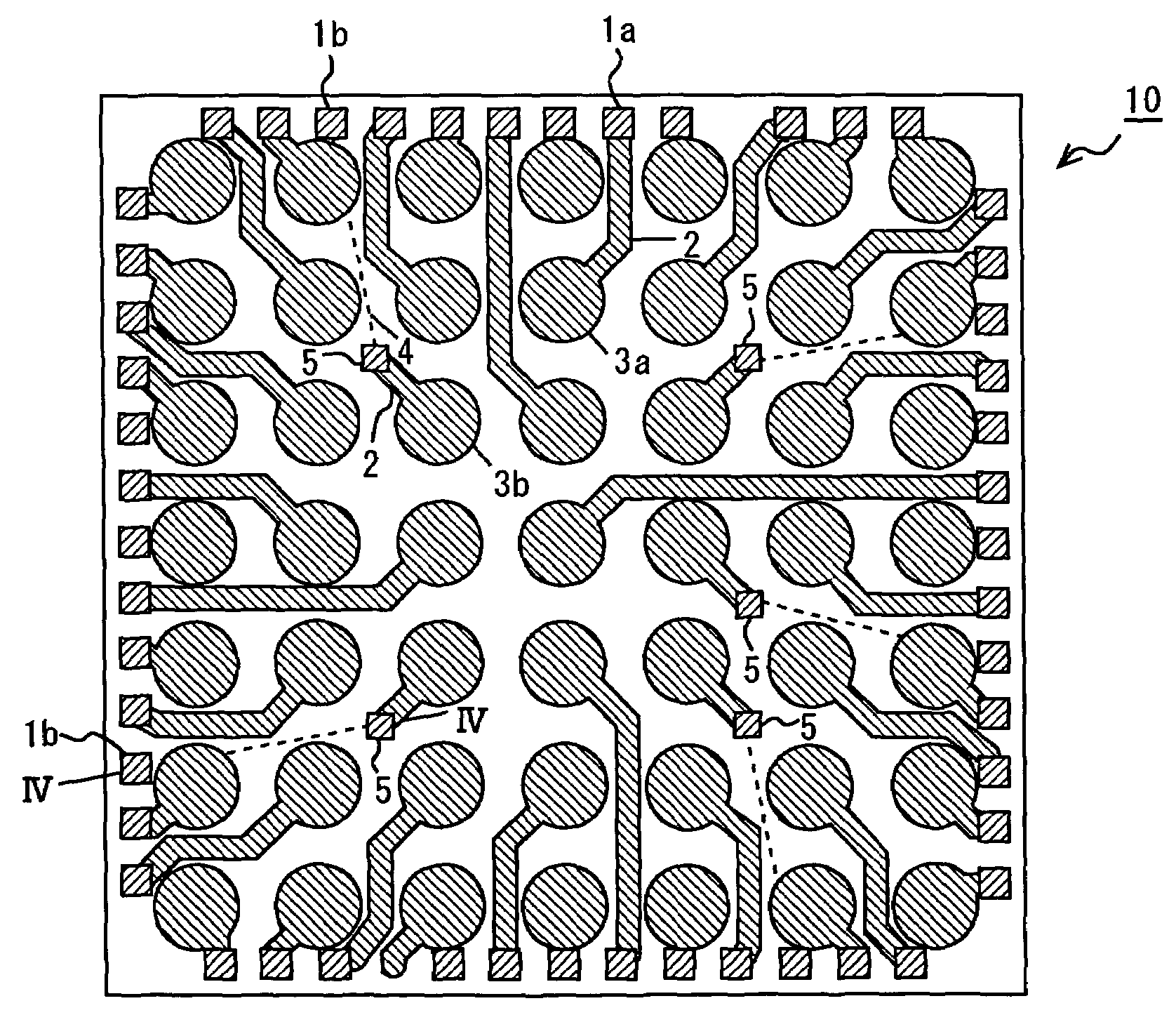
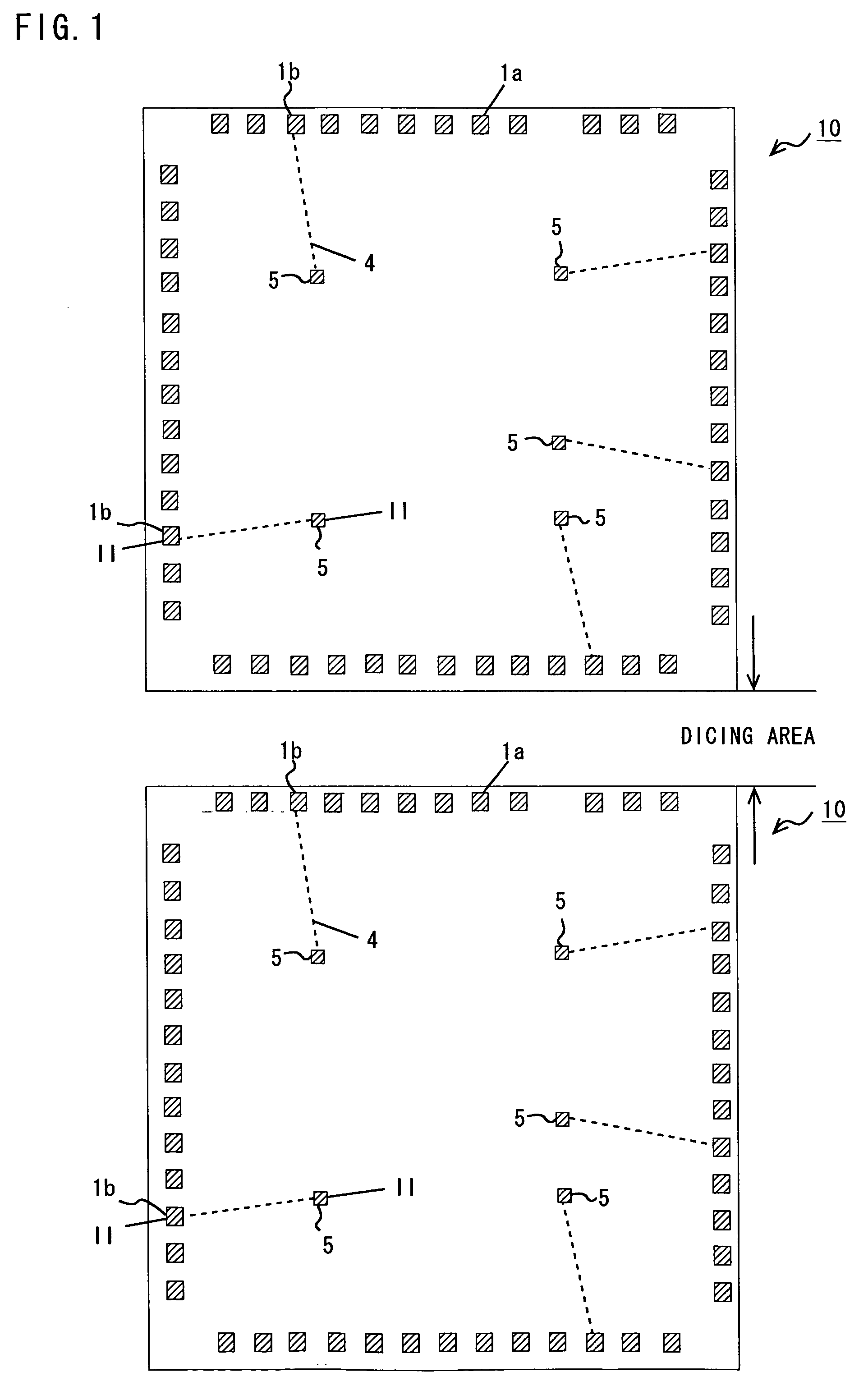
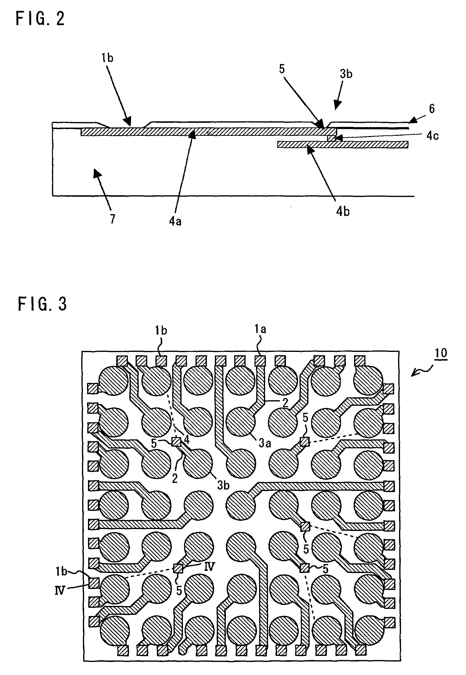
[0032]A semiconductor chip according to a preferred embodiment of the present invention will be explained hereinafter with reference to accompanying drawings. FIG. 1 shows an example of line arrangement of a semiconductor chip 10 before rewiring and land pad formation are performed. Two of the semiconductor chips 10 on a wafer are shown, and the space between the semiconductor chips 10 is a dicing area. The semiconductor chip 10 has a plurality of circuit blocks, for example. The circuit blocks include a CPU core, DSP core, analog circuit, analog-to-digital converter circuit, memories (ROM / RAM), and logic circuit.

[0033]As shown in FIG. 1, on the periphery of the semiconductor chip 10 are formed a plurality of peripheral electrode pads 1a and 1b that are peripheral electrodes. The peripheral electrode pads 1a and 1b are connected to various internal circuits (not shown) formed in the semiconductor chip 10 by internal lines (not shown). When inspecting the internal circuits of the sem...


PUM


Abstract

A semiconductor device has peripheral electrode pads formed on the periphery of a semiconductor chip, land pads comprising the first land pads and the second land pads formed on the semiconductor chip, and circuits formed in the semiconductor chip. The peripheral electrode pads are connected to internal circuits by internal lines. The first land pads are connected to the peripheral electrode pads by rewired lines. The second electrode pads, on the other hand, are connected to the internal circuits by internal electrode pads and internal lines, not by the peripheral electrode pads.

Description

CROSS-REFERENCE TO RELATED APPLICATION[0001]The present invention is related to Japanese Patent Application Serial No. 2003-020939. It is hereby incorporated.BACKGROUND OF THE DISCLOSURE[0002]1. Field of the Invention[0003]The present invention relates to semiconductor devices, and, more particularly, to arrangement of peripheral electrodes, internal electrodes, and internal lines of semiconductor chips.[0004]2. Description of the Related Art[0005]Demand for smaller, thinner, and lighter products is high in the area of electrical devices such as mobile phones, digital cameras, and notebook computers. Accordingly, development of smaller, thinner, and lighter semiconductor components used in the electrical devices with low production costs is an important subject for study.[0006]Recently, BGA (ball grid array) and CSP (Chip Scale Package or Chip Size Package) have been increasingly developed and already put into practical use in some cases. The BGA and CSP are smaller packages that re...

Claims


Application Information

Patent Timeline
IPC IPC(8): H01L23/52H01L23/48H01L29/40H01L21/3205H01L21/82H01L21/822H01L23/12H01L23/31H01L23/522H01L27/04
CPCH01L23/3114H01L23/522H01L24/05H01L24/06H01L2224/04042H01L2924/01033H01L24/48H01L2924/3011H01L2924/014H01L2924/01082H01L2924/01078H01L2924/01075H01L24/16H01L2224/0401H01L2224/05556H01L2224/16H01L2224/48227H01L2224/48465H01L2924/01004H01L2924/01005H01L2924/01006H01L2924/01013H01L2924/01014H01L2924/01015H01L2924/01029H01L2924/01057H01L2924/00014H01L2924/00H01L2224/023H01L2224/05599H01L2224/45099H01L2224/85399H01L2924/181H01L2924/00012H01L2224/45015H01L2924/207H01L2924/0001
Inventor KANAI, TOMONORIKISHIMOTO, KIYOHARUKIKUCHI, YUJI
Owner MAXELL HLDG LTD
Why Eureka
Try Eureka