Method of manufacturing semiconductor light emitting device

a technology of light-emitting devices and semiconductors, which is applied in the direction of semiconductor devices, lasers, semiconductor lasers, etc., can solve the problems of reducing the thermal saturation level and the tapered shape starts to have some drawbacks, so as to prevent the width of the bottom section of the groove from becoming extremely small, the thermal saturation level and the kink level can be improved, and the effect of excelling in isotropy

Inactive Publication Date: 2007-04-24
SONY CORP
View PDF6 Cites 10 Cited by
  • Summary
  • Abstract
  • Description
  • Claims
  • Application Information

AI Technical Summary

Benefits of technology

[0019]In accordance with the first and the second methods of manufacturing a semiconductor light emitting device according to embodiments of the present invention, the upper section groove of the ridge groove is formed by etching, which maintains the verticality of the ridge by employing the anisotropic etching. Accordingly, the width of the ridge section formed between the ridge grooves can be set at a larger value. As a result, the thermal saturation level and the kink level can be improved.
[0020]Furthermore, the isotropic etching, i.e. wet etching is performed only on the bottom section of the ridge groove. Thus, the ridge groove having a predetermined depth can accurately be formed. Further, the etching, which excels in isotropy, is performed only on the bottom section of the ridge groove, within a limited depth. Accordingly, the width of the bottom section of the groove is prevented from becoming extremely small. Thus, the increase in the width W2 of the bottom section of the ridge can be suppressed. Consequently, the asymmetry in a spot shape of oscillating light, which is caused by the increase in the width W2 of the bottom section of the ridge, can be alleviated. In other words, unevenness of a radiation angle (θ / / ) of oscillating light can be mitigated.
[0021]Further, in accordance with the first method of manufacturing a semiconductor light emitting device according to the present embodiment, single etching stop layer is used. In accordance with the second method of manufacturing a semiconductor light emitting device according to the present embodiment, two etching stop layers are used. Accordingly, the progress of etching upwardly from the bottom section of the ridge at the anisotropic etching can effectively be suppressed. Thus, it is possible to assure advantageous effect of that the width W1 of the upper section of the ridge and the verticality thereof can be maintained.

Problems solved by technology

However, in recent years, due to demands for high output semiconductor lasers, this tapered shape starts to have some drawbacks.
Thus, the drawbacks associated with increase in the output thereof, such as carrier overflow, lowering of the thermal saturation level, and that of the kink level, have arisen.

Method used


Image

  • Method of manufacturing semiconductor light emitting device
  • Method of manufacturing semiconductor light emitting device
  • Method of manufacturing semiconductor light emitting device

Examples


first embodiment

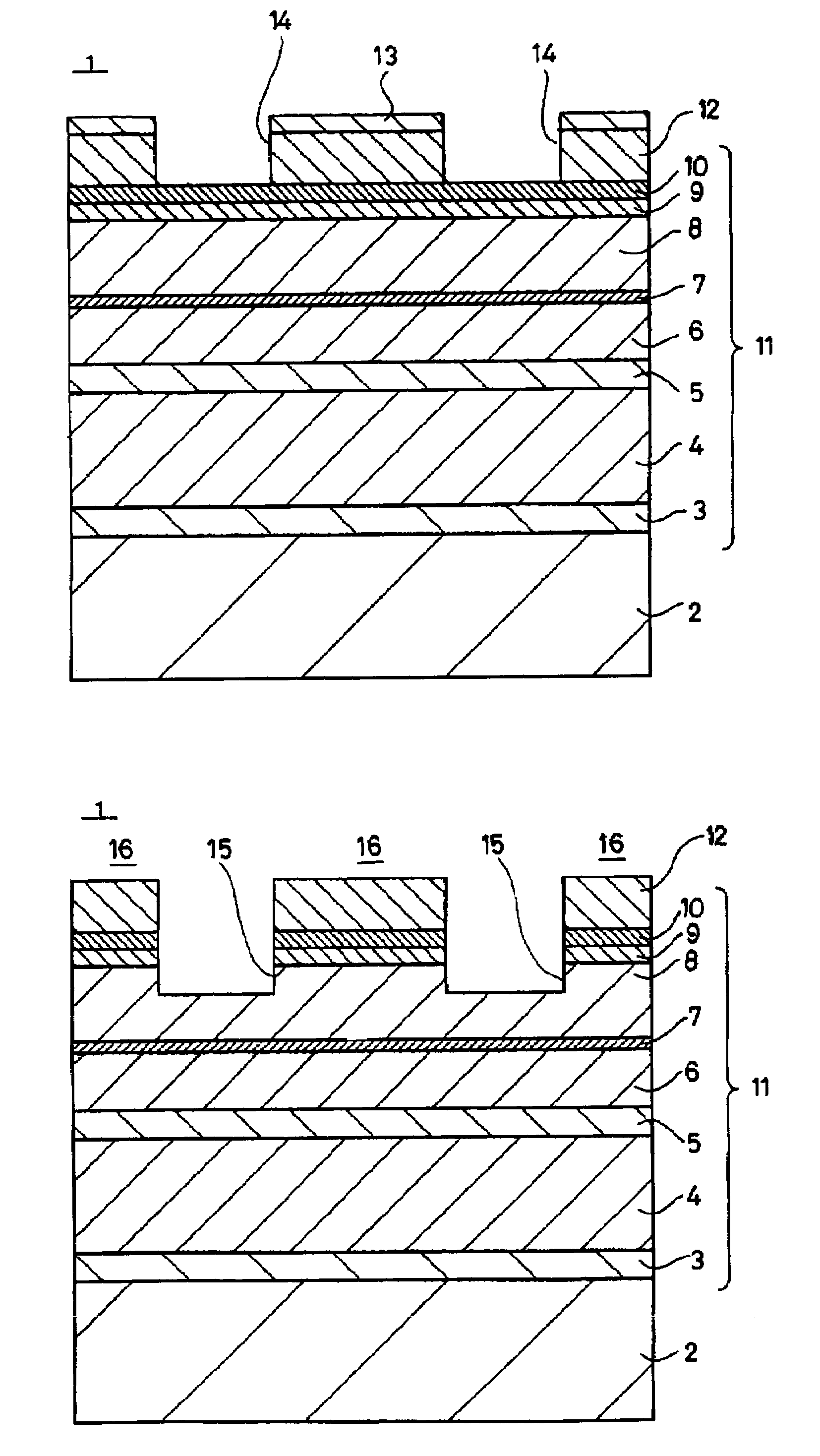
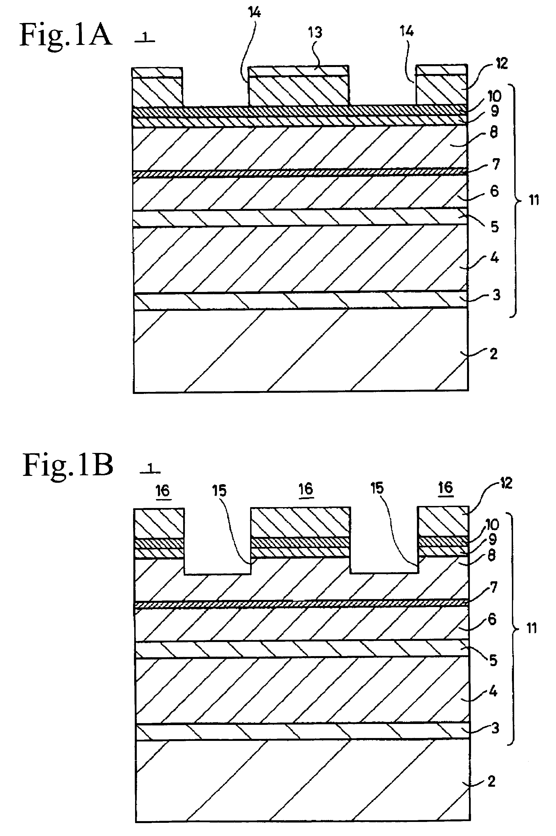
[0034]First, the first method of manufacturing a semiconductor light emitting device according to an embodiment of the present invention is described hereinbelow by referring to FIGS. 1 to 4, which are enlarged cross-sectional views illustrating processes of the first method.

[0035]In the present embodiment, first, a buffer layer 3 made of the first conductive type (for example, the n-type) GaInP, a cladding layer 4 made of the first conductive type (for instance, the n-type) AlGaInP, an active layer 5 of MQW (Multi-Quantum Well) structure made of, for example, GaInP and AlGaInP, a first cladding layer 6 made of the second conductive type (for instance, the p-type) AlGaInP, an etching stop layer 7 formed by repeating three times the formation of a 50 Å thick layer made of the second conductive type (for example, the p-type) GaInP and AlGaInP, a second cladding layer 8 made of the second conductive type (for instance, the p-type) AlGaInP, an intermediate layer 9 made of the second con...

second embodiment

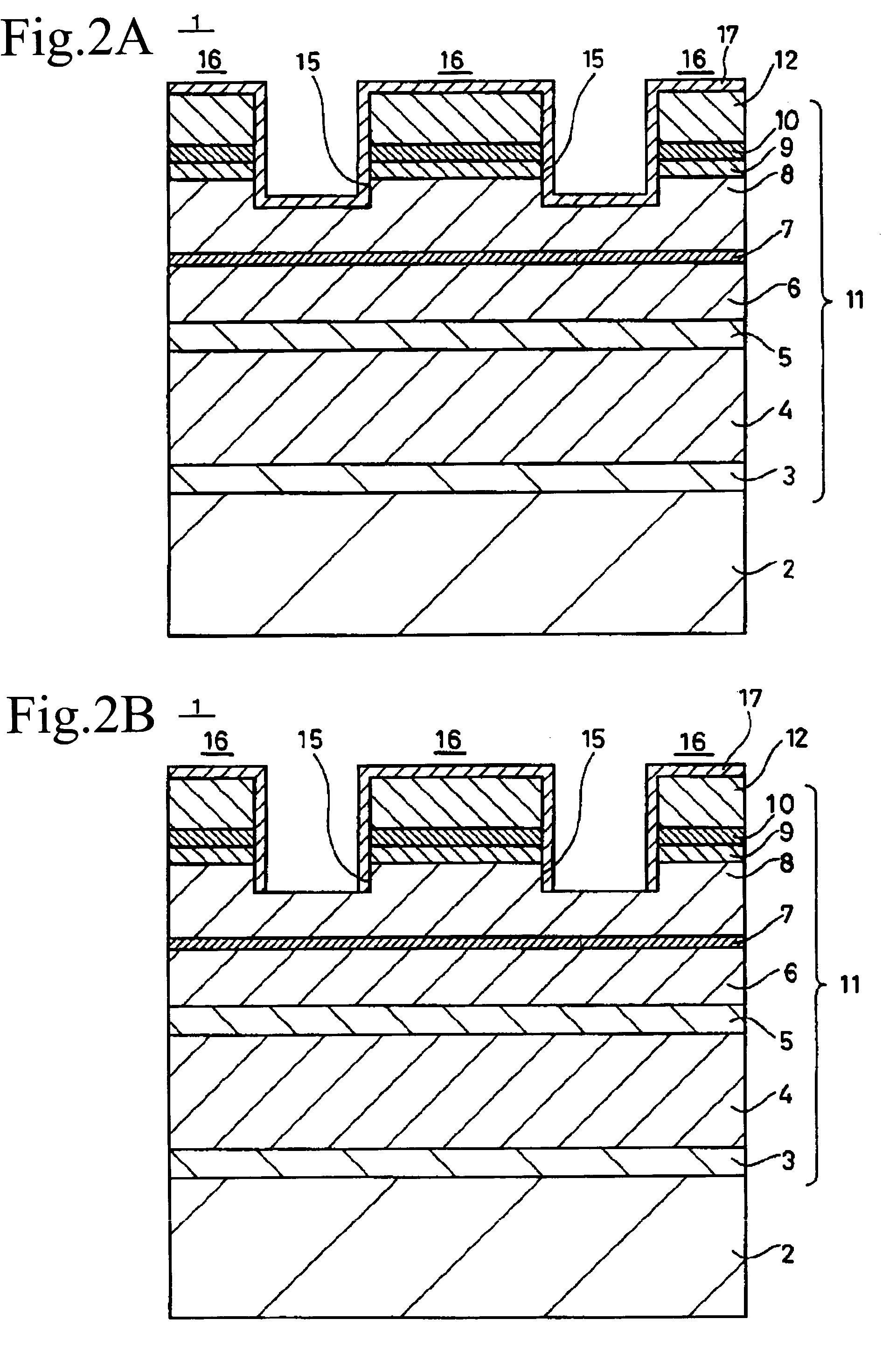
[0043]The second method of manufacturing a semiconductor light emitting device according to another embodiment of the present invention is described hereinbelow by referring to FIGS. 5 to 8, which are enlarged cross-sectional views illustrating processes of the second method.

[0044]In the present embodiment, first, a buffer layer 33 made of the first conductive type (for example, the n-type) GaInP, a cladding layer 34 made of the first conductive type (for instance, the n-type) AlGaInP, an active layer 35 of MQW (Multi-Quantum Well) structure made of, for example, GaInP and AlGaInP, a first cladding layer 36 made of the second conductive type (for instance, the p-type) AlGaInP, a first etching stop layer 37 formed by repeating three times the formation of a 50 Å thick layer made of the second conductive type (for example, the p-type) GaInP and AlGaInP, a second cladding layer 38 made of the second conductive type (for instance, the p-type) AlGaInP, a second etching stop layer 39 form...


PUM


Abstract

A method of manufacturing a ridge type semiconductor light emitting device includes: a process of epitaxially growing a multi-layered semiconductor layer having at least a first conductive type cladding layer, an active layer, a second conductive type first cladding layer, an etching stop layer, and a second conductive type second cladding layer on a substrate; a process of forming a ridge groove for forming a ridge; and a process of forming a current-flow barrier layer in the ridge groove. The process of forming ridge grooves has first and second anisotropic etching processes of performing anisotropic etching, an etching-mask forming process, and an isotropic etching process of performing anisotropic etching.

Description

CROSS REFERENCES TO RELATED APPLICATIONS[0001]The present invention claims priority to its priority document No. 2003-421378 filed in the Japanese Patent Office on Dec. 18, 2003, the entire contents of which being incorporated by reference herein.BACKGROUND OF THE INVENTION[0002]1. Field of the Invention[0003]The present invention relates to a method of manufacturing a semiconductor light emitting device whose thermal saturation level and kink level are improved, and more particularly to a method of manufacturing a semiconductor light emitting device having ridges, i.e. stripe sections constituting current paths.[0004]2. Description of the Related Art[0005]Hitherto, in the manufacture of semiconductor light emitting devices, for example, semiconductor lasers, grooves of desired shapes have often been formed (for example, see Japanese Patent Application Publication 2003-60307, Paragraph 0030).[0006]Usually, the formation of grooves is performed by anisotropic etching or isotropic etc...

Claims


Application Information

Patent Timeline
Patent Type & Authority Patents(United States)
IPC IPC(8): H01L21/00H01L29/22H01L33/00H01S5/223H01L21/302H01S5/20H01S5/22H01S5/343
CPCB82Y20/00H01S5/2231H01L33/005H01S5/2086H01S5/221H01S5/34326
Inventor CHIBA, MARIKUDO, HISASHIAGATSUMA, SHINICHI
Owner SONY CORP
Why Eureka
Try Eureka