Method for manufacturing printed circuit board
a manufacturing method and printed circuit board technology, applied in the direction of double resist layer, non-metallic protective coating application, conductive pattern formation, etc., can solve the problems of difficult abrading operation, conventional method of manufacturing printed circuit board, and large impact on product quality, so as to improve manufacturing efficiency and product yield
- Summary
- Abstract
- Description
- Claims
- Application Information
AI Technical Summary
Benefits of technology
Problems solved by technology
Method used
Image
Examples
first embodiment
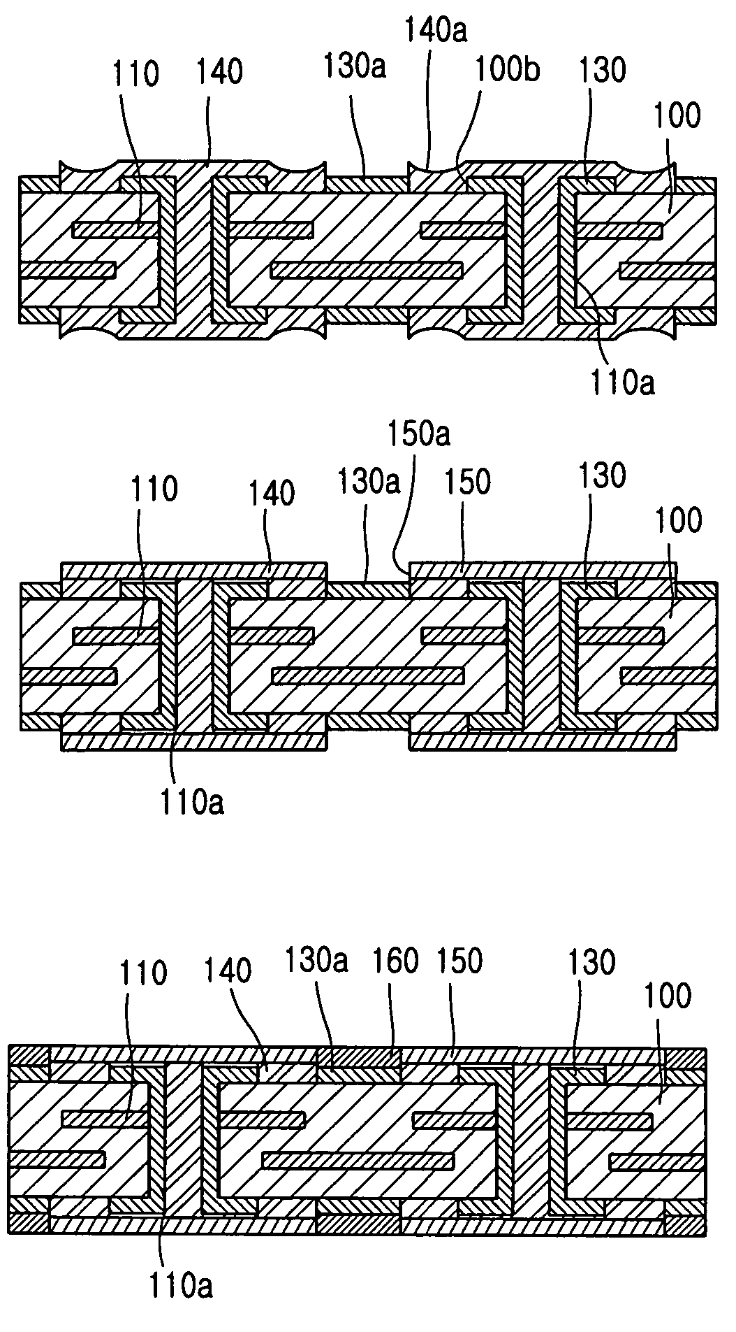
[0043]FIGS. 5A to 5G are longitudinal sectional views that sequentially show a method for manufacturing a printed circuit board in accordance with the present invention.
[0044]In the method for manufacturing a printed circuit board in accordance with the first embodiment of the present invention, as shown in FIG. 5A, inner circuit patterns 110 are formed in an insulating material 100 in multi-layers, and a plurality of through holes 100a are formed at certain portions of the insulating material 100.
[0045]Then, as shown in FIG. 5B, a copper sheet 110a is formed inside the through hole 100a to electrically connect the inner circuit pattern 110 and an outer circuit pattern 130 to be described later.
[0046]An outer circuit pattern 130 is formed at an inner circumferential surface of the through hole 100a and a surface of the insulating material 100 and electrically connected to the inner circuit pattern 110. Then, a specific portion of the outer circuit pattern 130 is exposed to light and...
second embodiment
[0060]In the method for manufacturing a printed circuit board in accordance with the present invention, as shown in FIG. 6A, inner circuit patterns 210 are formed in an insulating material 200 in multi-layers, a plurality of through holes 200a are formed at certain portions of the insulating material 200.
[0061]Then, as shown in FIG. 6B, a copper sheet 210a is formed inside the through hole 200a to electrically connect the inner circuit pattern 210 and an outer circuit pattern 230 to be described later.
[0062]An outer circuit pattern 230 is formed at an inner circumferential surface of the through hole 200a and a surface of the insulating material 200 and electrically connected to the inner circuit pattern 210. Then, a specific portion of the outer circuit pattern 230 is exposed to light and developed to be removed.
[0063]Then, as shown in FIG. 6C, to protect the outer circuit pattern 230, a first photo solder resist layer 240 is formed at an entire surface of the insulating material a...
PUM
| Property | Measurement | Unit |
|---|---|---|
| photosensitive | aaaaa | aaaaa |
| depth | aaaaa | aaaaa |
| height | aaaaa | aaaaa |
Abstract
Description
Claims
Application Information


