Growth of planar reduced dislocation density m-plane gallium nitride by hydride vapor phase epitaxy

a gallium nitride and dislocation density technology, applied in the direction of single crystal growth, polycrystalline material growth, chemistry apparatus and processes, etc., can solve the undesirable quantum-confined stark effect of conventional c-plane quantum well structure in iii-nitride based optoelectronic and electronic devices, qcse, red-shifted emission, etc., to achieve the effect of reducing the density of structural defects

Inactive Publication Date: 2007-04-24
JAPAN SCI & TECH CORP
View PDF30 Cites 114 Cited by
  • Summary
  • Abstract
  • Description
  • Claims
  • Application Information

AI Technical Summary

Benefits of technology

[0025]The present invention provides a method of growing highly planar, fully transparent and specular m-plane GaN films. The method provides for a significant reduction in structural defect densities via a lateral overgrowth technique. High quality, uniform, thick m-plane GaN films are produced for use as substrates for polarization-free device growth.

Problems solved by technology

However, conventional c-plane quantum well structures in III-nitride based optoelectronic and electronic devices suffer from the undesirable quantum-confined Stark effect (QCSE), due to the existence of strong piezoelectric and spontaneous polarizations.
The strong built-in electric fields along the c-direction cause spatial separation of electrons and holes that in turn give rise to restricted carrier recombination efficiency, reduced oscillator strength, and red-shifted emission.
Bulk crystals of GaN are not available so it is not possible to simply cut a crystal to present a surface for subsequent device regrowth.
One significant disadvantage of heteroepitaxial growth of nitrides is that structural defects are generated at the interface between the substrate and epitaxial film.
The two predominant types of extended defects of concern are threading dislocations and stacking faults.
However, to date no such process has been developed or demonstrated for m-plane GaN.

Method used


Image

  • Growth of planar reduced dislocation density m-plane gallium nitride by hydride vapor phase epitaxy
  • Growth of planar reduced dislocation density m-plane gallium nitride by hydride vapor phase epitaxy
  • Growth of planar reduced dislocation density m-plane gallium nitride by hydride vapor phase epitaxy

Examples


Embodiment Construction

[0035]In the following description of the preferred embodiment, reference is made to the accompanying drawings which form a part hereof, and in which is shown by way of illustration a specific embodiment in which the invention may be practiced. It is to be understood that other embodiments may be utilized and structural changes may be made without departing from the scope of the present invention.

[0036]Overview

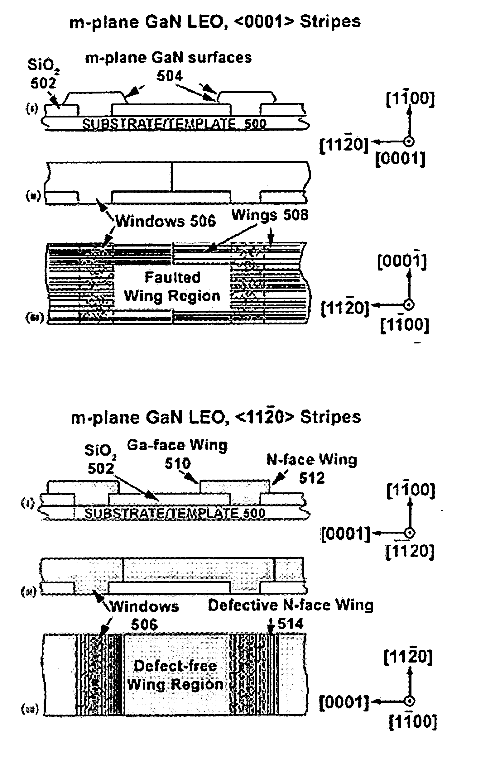
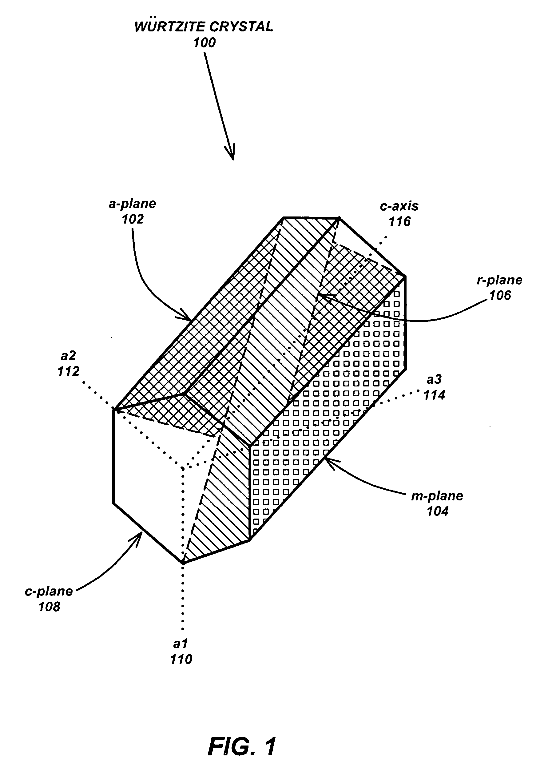
[0037]Growth of non-polar m-plane {1 100} nitride semiconductors offers a means of eliminating polarization effects in würtzite-structure III:nitride device structures. Current (Ga,Al,In,B)N devices are grown in the polar [0001] c-direction, which results in charge separation along the primary conduction direction in optoelectronic devices. The resulting polarization fields are detrimental to the performance of current state of the art devices. Growth of these devices along a non-polar direction could improve device performance significantly.

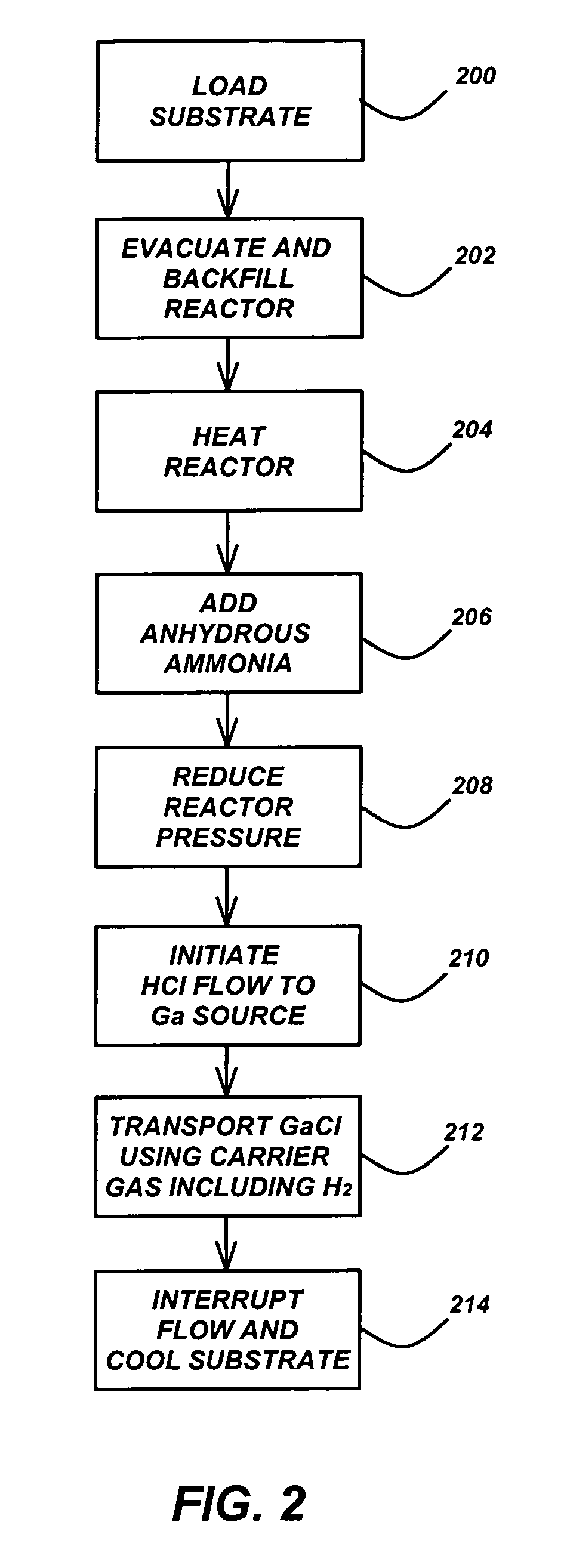
[0038]Previous efforts to grow thic...


PUM

PropertyMeasurementUnit
thickaaaaaaaaaa
temperatureaaaaaaaaaa

Abstract

A method of growing highly planar, fully transparent and specular m-plane gallium nitride (GaN) films. The method provides for a significant reduction in structural defect densities via a lateral overgrowth technique. High quality, uniform, thick m-plane GaN films are produced for use as substrates for polarization-free device growth.

Description

CROSS-REFERENCE TO RELATED APPLICATIONS[0001]This application claims the benefit under 35 U.S.C. Section 119(e) of the following co-pending and commonly-assigned U.S. patent application:[0002]U.S. Provisional Patent Application Ser. No. 60 / 576,685, filed on Jun. 3, 2004, by Benjamin A. Haskell, Melvin B. McLaurin, Steven P. DenBaars, James S. Speck, and Shuji Nakamura, entitled “GROWTH OF PLANAR REDUCED DISLOCATION DENSITY M-PLANE GALLIUM NITRIDE BY HYDRIDE VAPOR PHASE EPITAXY,”[0003]which application is incorporated by reference herein.[0004]This application is a continuation-in-part and claims the benefit under 35 U.S.C. Sections 119, 120 and / or 365 of the following co-pending and commonly-assigned patent applications:[0005]International Patent Application No. PCT / US03 / 21918, filed Jul. 15, 2003, by Benjamin A. Haskell, Michael D. Craven, Paul T. Fini, Steven P. DenBaars, James S. Speck, and Shuji Nakamura, entitled “GROWTH OF REDUCED DISLOCATION DENSITY NON-POLAR GALLIUM NITRIDE ...

Claims


Application Information

Patent Timeline
Patent Type & Authority Patents(United States)
IPC IPC(8): H01L21/36H01L21/20C30B25/02C30B29/40H01L21/00H01L21/205H01L21/31H01L21/469
CPCC30B25/02C30B29/406H01L21/02378H01L21/0242H01L21/02458H01L21/0254H01L21/02609H01L21/02639H01L21/02647C30B29/40H01L21/02433H01L21/0262H01L21/02642
Inventor HASKELL, BENJAMIN A.MCLAURIN, MELVIN B.DENBAARS, STEVEN P.SPECK, JAMES STEPHENNAKAMURA, SHUJI
Owner JAPAN SCI & TECH CORP
Why Eureka
Try Eureka