

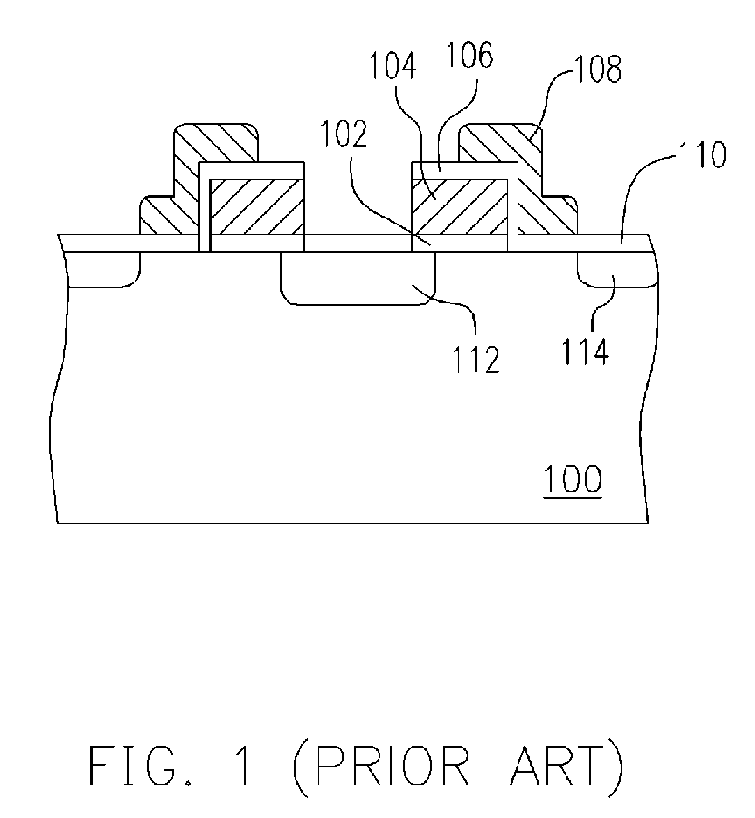
Split gate flash memory
a technology of split gate and flash memory, which is applied in the field of split gate flash memory, can solve the problems of inability to integrate devices at a level that is difficult to achieve, the size of each memory cell must increase, and the error in reading from the flash memory may occur, so as to achieve the effect of increasing the level of integration of memory devices and prolonging the channel length
- Summary
- Abstract
- Description
- Claims
- Application Information
AI Technical Summary
Benefits of technology
Problems solved by technology
Method used
Image

Examples
Embodiment Construction
[0048]Reference will now be made in detail to the present preferred embodiments of the invention, examples of which are illustrated in the accompanying drawings. Wherever possible, the same reference numbers are used in the drawings and the description to refer to the same or like parts.
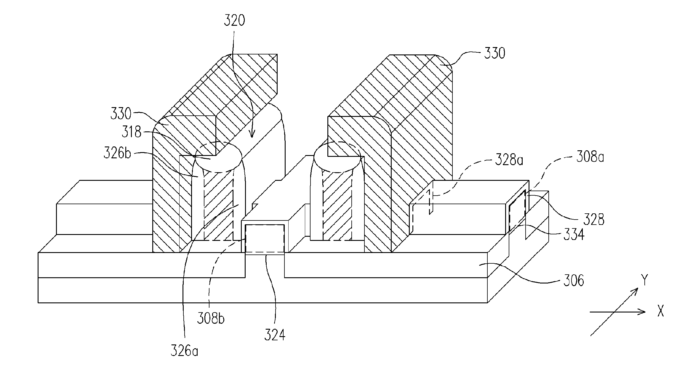
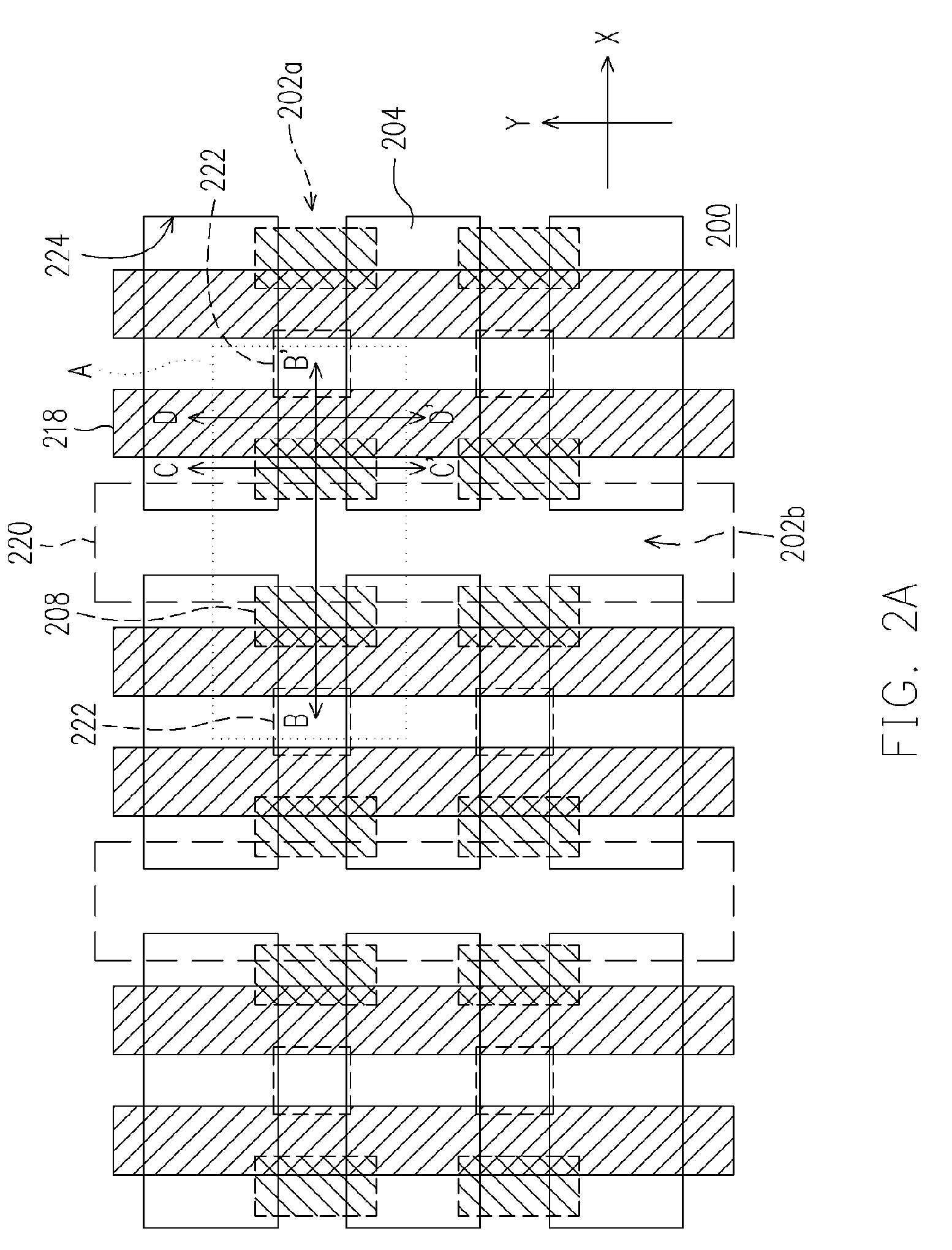
[0049]FIG. 2A is a top view of a split gate flash memory according to one preferred embodiment of the present invention. FIG. 2B is a perspective view showing the ‘A’ portion of the structure in FIG. 2A. FIG. 2C is a cross-sectional view showing the structure along line B–B′ of FIG. 2A. FIG. 2D is a cross-sectional view showing the structure along line C–C′ of FIG. 2A. FIG. 2E is a cross-sectional view showing the structure along line D–D′ of FIG. 2A.
[0050]FIGS. 2A through 2E are used to describe the structure of a split gate flash memory according to the present invention. The flash memory cell of the present invention includes at least a substrate 200, an active layer 202a, another active layer 202...
PUM
 Abstract
Description
Claims
Application Information