Current load device and method for driving the same

Active Publication Date: 2007-04-24
HANNSTAR DISPLAY CORPORATION
View PDF6 Cites 64 Cited by
  • Summary
  • Abstract
  • Description
  • Claims
  • Application Information

AI Technical Summary

Benefits of technology

[0022]According to the arrangement of this invention described above, a switch is provided between the driving transistor for retaining and supplying the current and the current load element, and the switch is held in the of f state during a period of operation of retaining the current; that operation is to set a gate voltage of the driving TFT to flow an appropriate current between the drain and the source of the driving TFT via the signal line. Therefore, in retaining the current, the effect of the capacitance of the current load element can be eliminated and the current can be retained in a short time.
[0023]Besides, in the case of an arrangement in which the switch SW between the driving transistor for retaining and supplying the current and the current load element is turned off an arbitrary time after the start of the supply of the current to the current load element, the performance of the current load element becomes the time-average

Problems solved by technology

The first conventional example has a disadvantage.
Consequently, the light emitting devices are not supplied with a current enough to provide an expected brightness, and thus, the quality of the display device is reduced.
In particular, there is quite large deviation of current/voltage characteristics of poly-silicon TFTs, which are often used in display devices, so that the image quality thereof is significantly reduced.
However, there is quite large deviation of current/voltage characteristics of poly-silicon TFTs, and even if the same voltage is applied to the gates of TFTs, the light emitting devices are supplied with various currents, and thus, the brightness thereof varies.
Therefore, there is a disadvantage that it is difficult to cause the light emitting device to emit light with an intended brightness, and the quality of the display device is reduced.
However, unlike with a crystalline silicon transistor, it is possible that the transistors of the pair

Method used


Image

  • Current load device and method for driving the same
  • Current load device and method for driving the same
  • Current load device and method for driving the same

Examples


first embodiment

[First Embodiment]

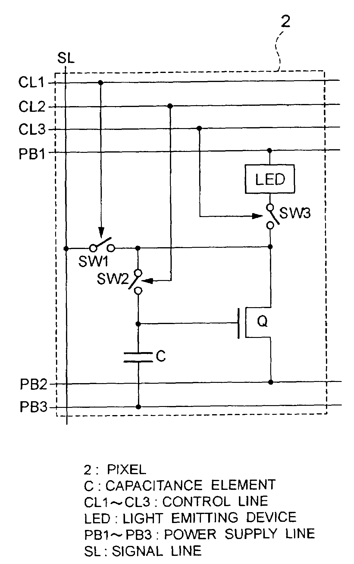
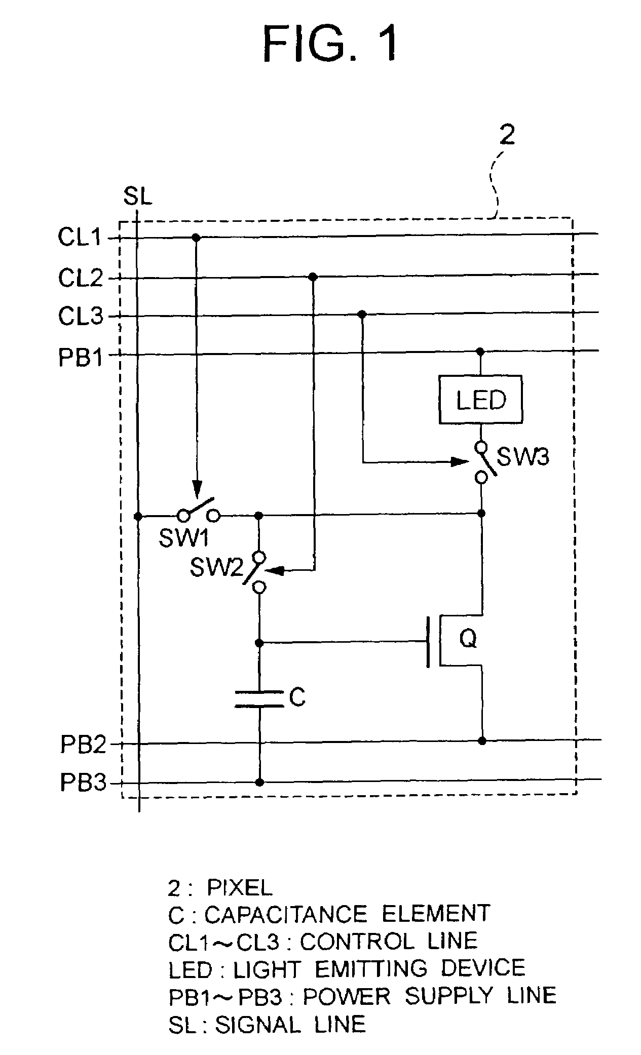
[0066]FIG. 1 is a circuit diagram showing a configuration of one pixel according to a first embodiment of this invention. As shown in FIG. 1, a signal line SL extending in a column direction, control lines CL1 to CL3 extending in a row direction and voltage supply lines PB1 to PB3 run through a pixel 2, and a TFT Q, switches SW1 to SW3, a capacitance element C and a light emitting device LED are arranged in the pixel 2. A first terminal of the TFT Q, which is one of the drain or source thereof, is connected to the voltage supply line PB2, the switch SW3 is connected between a second terminal of the TFT Q, which is the other of the drain or source thereof, and the light emitting device LED, and the switch SW1 is connected between the second terminal of the TFT Q and the signal line SL. A terminal of the light emitting device LED on the other side of the switch SW3 is connected to the voltage supply line PB1. The switch SW2 is connected between the second terminal an...

second embodiment

[Second Embodiment]

[0082]FIG. 5 is a circuit diagram showing a configuration of one pixel according to a second embodiment of this invention. As shown in FIG. 5, a signal line SL extending in a column direction, control lines CL1 to CL3 extending in a row direction and voltage supply lines PB1 to PB3 run through a pixel 2, and a TFT Q, switches SW1 to SW3, a capacitance element C and a light emitting device LED are arranged in the pixel 2. A first terminal of the TFT Q, which is one of the drain or source thereof, is connected to the voltage supply line PB2, the switch SW3 is connected between a second terminal of the TFT Q, which is the other of the drain or source thereof, and the light emitting device LED, and the switch SW1 is connected between the second terminal of the TFT Q and the signal line SL. A terminal of the light emitting device LED on the other side of the switch SW3 is connected to the voltage supply line PB1. The switch SW2 is connected between the signal line SL a...

third embodiment

[Third Embodiment]

[0089]FIG. 7 is a circuit diagram showing a configuration of one pixel according to a third embodiment of this invention. As shown in FIG. 7, a signal line SL extending in a column direction, control lines CL1 to CL3 extending in a row direction and voltage supply lines PB1 to PB3 and PB5 run through a pixel 2, and a TFT Q1, a TFT Q2, switches SW1 to SW3, a capacitance element C and a light emitting device LED are arranged in the pixel 2. The TFT Q1 and the TFT Q2 are connected in series, one of the drain and source of the TFT Q2, which is not connected to the TFT Q1, is connected to the voltage supply line PB2, the switch SW3 is connected between the light emitting device LED and one of the drain and source of the TFT Q1, which is not connected to the TFT Q2, and the switch SW1 is connected between the signal line SL and the terminal of the TFT Q1, which is not connected to the TFT Q2. A terminal of the light emitting device LED on the other side of the switch SW3...


PUM


Abstract

This invention provides a precise current load device. A cell includes a power supply line, a ground line, first and second voltage supply lines, a signal line, first, third and fourth control lines, first to fourth switches, a p-type TFT, a capacitance element, and a current load element. A source of the p-type TFT is connected to the power supply line, one terminal of the current load element is connected to the ground line, the first switch is connected between the signal line and a drain of the p-type TFT, the second switch is connected between the drain and the gate of the p-type TFT, the third switch is connected between the drain of the p-type TFT and the current load element, and the fourth switch is connected between the voltage supply line and the current load element.

Description

BACKGROUND OF THE INVENTION[0001]1. Field of the Invention[0002]The present invention relates to a current load driving circuit for driving a current load element and a method for driving the same. In particular, it relates to a current load device comprising current load elements and current load driving circuits arranged in a matrix, and a method for driving the same.[0003]2. Description of the Prior Art[0004]In recent years, a device having cells arranged in a matrix, each of the cells comprising a current load element that operates depending on a current passing therethrough and a current load driving circuit for driving the current load, has been developed.[0005]For example, in many light emitting display devices with an organic EL (electroluminescence) device serving as the current load element, pixels each comprising the organic EL device and a drive circuit therefor are arranged in a matrix and driven according to the active matrix method. FIG. 37 is a schematic plan view of...

Claims


Application Information

Patent Timeline
IPC IPC(8): G09G3/30G09G3/32H03K17/041
CPCG09G3/3233H03K17/04106G09G2300/0842G09G2300/0861G09G2310/0251G09G2310/0262G09G2320/0252
Inventor ABE, KATSUMI
Owner HANNSTAR DISPLAY CORPORATION
Why Eureka
Try Eureka