High fill-factor bulk silicon mirrors

a bulk silicon mirror and filling factor technology, applied in the field of microelectromechanical systems, can solve the problems of limiting the amount of surface area available for optical beam manipulation, arrays susceptible to misalignment and other undesirable effects, and achieve the effect of high optical fill factor, substantial rotational range, and maximized optical surface area of bulk elements

Inactive Publication Date: 2007-04-24
CAPELLA PHOTONICS INC
View PDF24 Cites 29 Cited by
  • Summary
  • Abstract
  • Description
  • Claims
  • Application Information

AI Technical Summary

Benefits of technology

[0016]One advantage of the MEMS apparatus of the invention is that by placing the hinge elements on an opposite side of the bulk element from the optical surface, and in a different plane from either the bulk element or the support layer, the optical surface area of the bulk element can be maximized and the entire optical surface becomes usable, e.g., for optical beam manipulation. This structure is highly advantageous for making arrayed MEMS devices, such as an array of MEMS mirrors with a high optical fill factor. Further, by advantageously using both bulk and surface micromachining techniques, a MEMS mirror according to the invention is characterized by a large and flat mirror along with flexible hinges, and is capable of achieving a substantial rotational range at moderate electrostatic drive voltages. An additional advantage of the MEMS apparatus of the invention is its monolithic structure, rendering it robust in performance. These advantageous features are in notable contrast with the prior devices.

Problems solved by technology

A notable shortcoming of this system is evident in that the thin-film hinges extend from the reflective surface side of the mirror to the frame, hence restricting (or obstructing) the amount of surface area available for optical beam manipulation.
In addition to the mirror plates being made of polysilicon (or thin-film), another drawback of the mirror array is the lack of a monolithic structure, which makes the array susceptible to misalignment and other extraneous undesirable effects.

Method used


Image

  • High fill-factor bulk silicon mirrors
  • High fill-factor bulk silicon mirrors
  • High fill-factor bulk silicon mirrors

Examples


first embodiment

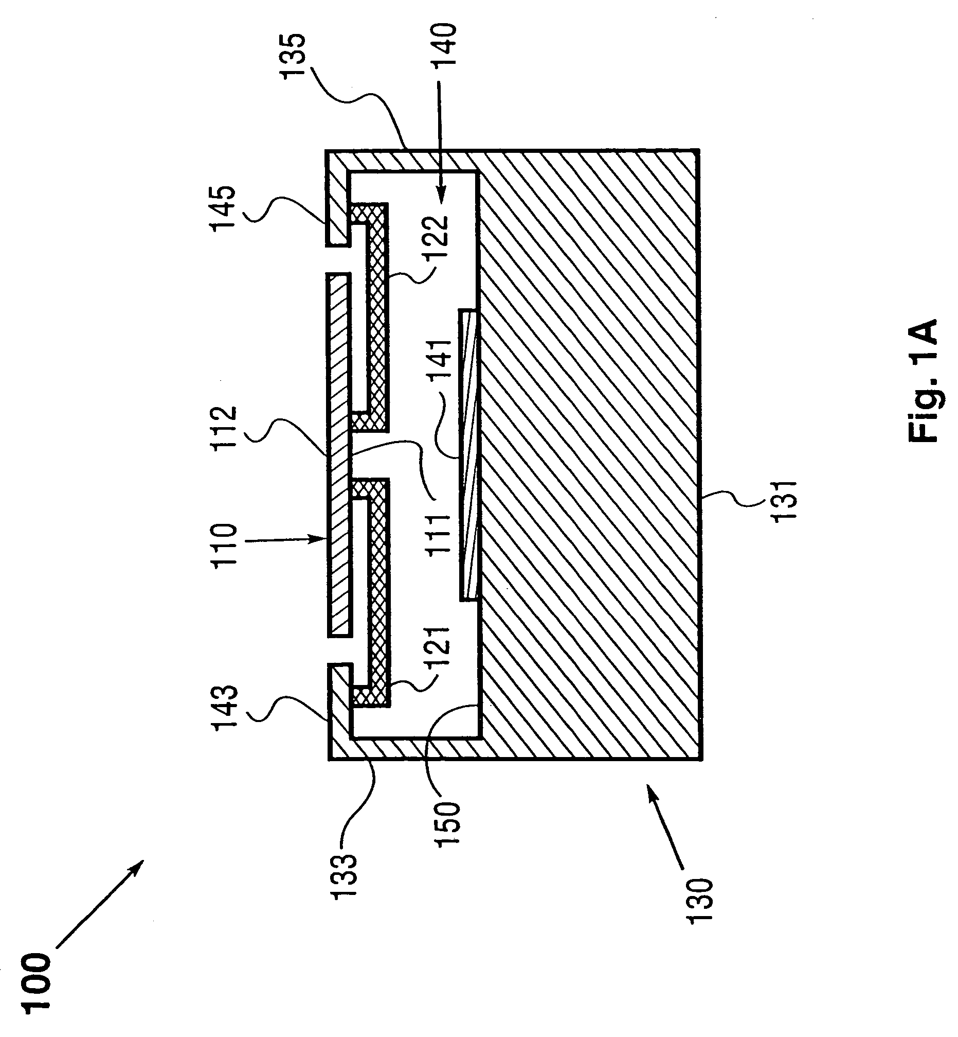
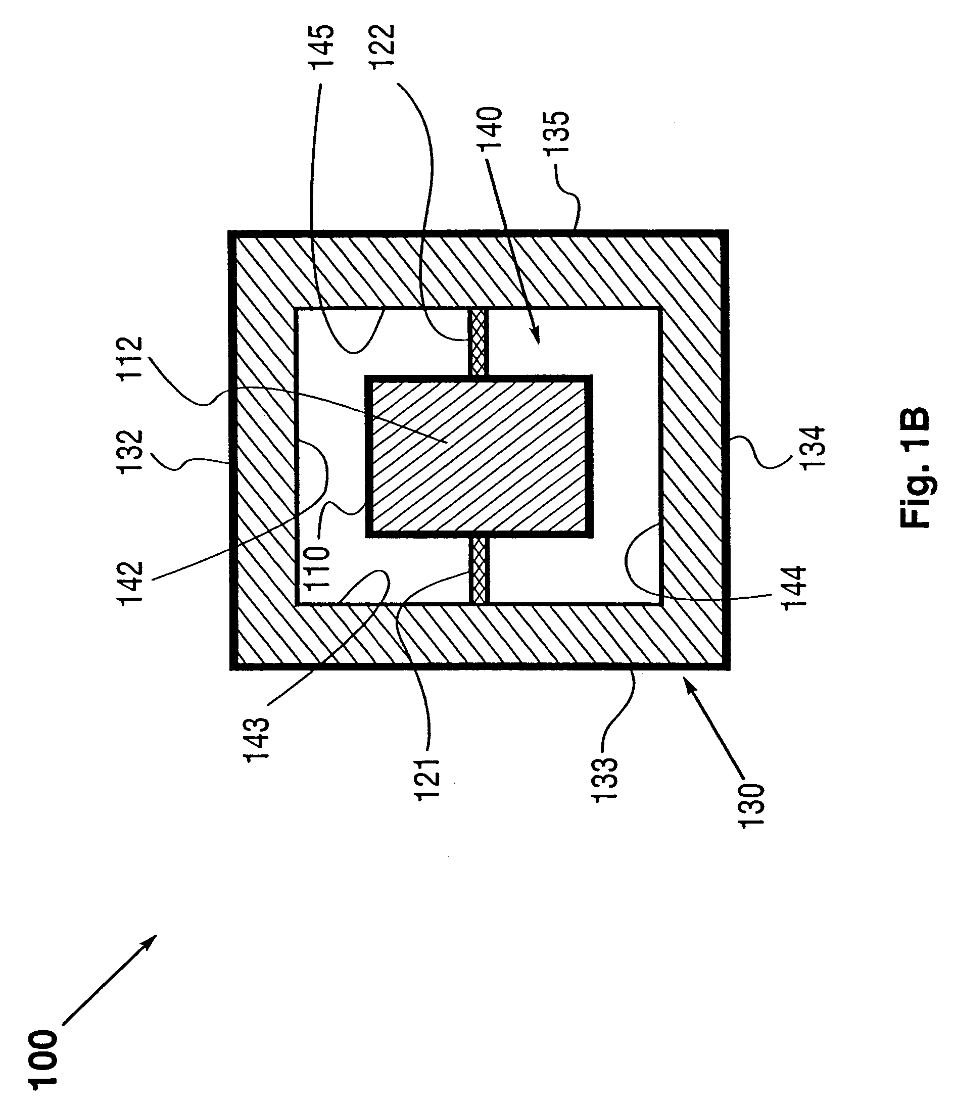
[0034]FIGS. 1A–1B illustrate a MEMS apparatus 100, according to the invention. FIG. 1A depicts a cross-sectional side view of the MEMS apparatus 100, which may comprise a bulk element 110, first and second hinge elements 121, 122, and a base support 130. The bulk element 110 may have a device (or “top” in the figures) surface 112, which may be substantially planar, and a “bottom” surface 111 that is disposed below the device surface 112 and on an opposite side of the bulk element. The device surface may be an optical surface, as described more fully herein. The first and second hinge elements 121, 122 may be disposed below the device surface 112, as shown. By way of example, in the embodiment of FIG. 1A, the hinge elements 121, 122 may be coupled to the bottom surface 111 of the bulk element 110 and to the base support 130 to attach or couple the bulk element to the base support. In this manner, the bulk element 110 is suspended from the support by the hinge elements 121, 122 with t...

second embodiment

[0038]FIG. 2 shows a cross-sectional side view of a MEMS apparatus in accordance with the invention, which affords a larger device surface area, i.e., higher fill factor, than the embodiment of FIGS. 1A–1B. By way of example, MEMS apparatus 200 may comprise a bulk element 210, first and second hinge elements 221, 222, and a base support 230. The bulk element 210 may include a substantially planar “device” (or “top”) surface 212, and a “bottom” surface 211 which is disposed below and on an opposite side of the bulk element from the device surface 212. In this embodiment, the bulk element 210 may further include a base portion 215, which may extend downward (in the figure) from the bottom surface 211. First and second hinge elements 221, 222 may be each disposed below the device surface 212 and coupled to the base portion or post 215 of the bulk element 110 and to the base support 130. In this manner, the bulk element 210 is suspended from the support with the hinge elements 221, 222 ...

third embodiment

[0041]FIG. 3 shows a cross-sectional side view of a MEMS apparatus 300 in accordance with the invention which also has a higher fill factor than the apparatus of FIGS. 1A–1B. With the exception of a bulk element 310, MEMS apparatus 300 is substantially similar to the MEMS apparatus 200, and may have the general configuration of and similar elements to those of the embodiment shown in FIG. 2. As shown in FIG. 3, the MEMS apparatus 300 may comprise a bulk element 310, first and second hinge elements 321, 322, and a base support 330. The base support 330 may include a cavity 340, which is formed by at least two sidewalls 333, 335 that extend from substrate portion 331. The cavity 340 may include a bottom surface 350, on which at least one electrode 341 may be disposed.

[0042]In the MEMS apparatus 300, the bulk element 310 may include a substantially planar device (or optical) top (in the FIG.) surface 312, and a bottom surface 311 which is disposed below and opposes the device surface 3...


PUM


Abstract

A method and apparatus for fabricating a MEMS apparatus having a device layer with an optical surface that is supported by a pedestal on a planar support layer that is suspended for movement with respect to a base support by hinge elements disposed in a different plane from the planar support layer. The surface area of the optical surface is maximized with respect to the base support to optimized the fill factor of the optical surface and afford a high passband. The height of the pedestal is selected to position the device layer sufficiently above the base support to afford an unobstructed predetermined angular rotation about each axis. The hinges may be made of thin-film material, fabricated by way of surface micromachining techniques. The hinges are disposed underneath the device layer enabling the optical surface to be maximized so that the entire surface becomes usable (e.g., for optical beam manipulation). MEMS devices afford an array of MEMS mirrors with a high optical fill factor and high passband. Further, use of both bulk and surface micromachining techniques gives a MEMS device with a large and flat mirror and flexible hinges capable of a substantial rotational range at modest electrostatic drive voltages.

Description

CROSS-REFERENCE TO RELATED APPLICATIONS[0001]This application is a continuation-in-part of application Ser. No. 10 / 159,153, filed May 31, 2002, now U.S. Pat. No. 6,695,457 which claims the benefit of U.S. Provisional Patent Application No. 60 / 295,682, filed on 2 Jun. 2001.BACKGROUND OF THE INVENTION[0002]This invention relates generally to micro-electro-mechanical systems (MEMS), and more particularly to MEMS apparatus and methods for making MEMS apparatus, such as mirrors, as by a combination of bulk and surface micromachining techniques.[0003]MEMS apparatus, such as mirrors, have utility in a variety of optical applications, including high-speed scanning and optical switching. In such applications, it is essential for MEMS mirrors to have flat optical surfaces, large rotational range, and robust performance.[0004]Many of these optical applications, e.g., optical networking applications, further require that MEMS mirrors be configured in a closely packed array. It is desirable in s...

Claims


Application Information

Patent Timeline
Patent Type & Authority Patents(United States)
IPC IPC(8): G02B26/08
CPCG02B26/0841Y10S359/904
Inventor VAN DRIEENHUIZEN, BERT P.DAVIS, JOSEPH E.
Owner CAPELLA PHOTONICS INC
Why Eureka
Try Eureka