Apparatus for radio telecommunication system and method of building up output power
a radio telecommunication system and apparatus technology, applied in the field of apparatus for radio telecommunication system and method of building up output power, can solve the problems of long time taken, difficult to build difficulty in building up output power within a prescribed time, so as to achieve rapid increase of control voltage
- Summary
- Abstract
- Description
- Claims
- Application Information
AI Technical Summary
Benefits of technology
Problems solved by technology
Method used
Image
Examples
second embodiment
[0055]FIG. 6 illustrates a precharge circuit.
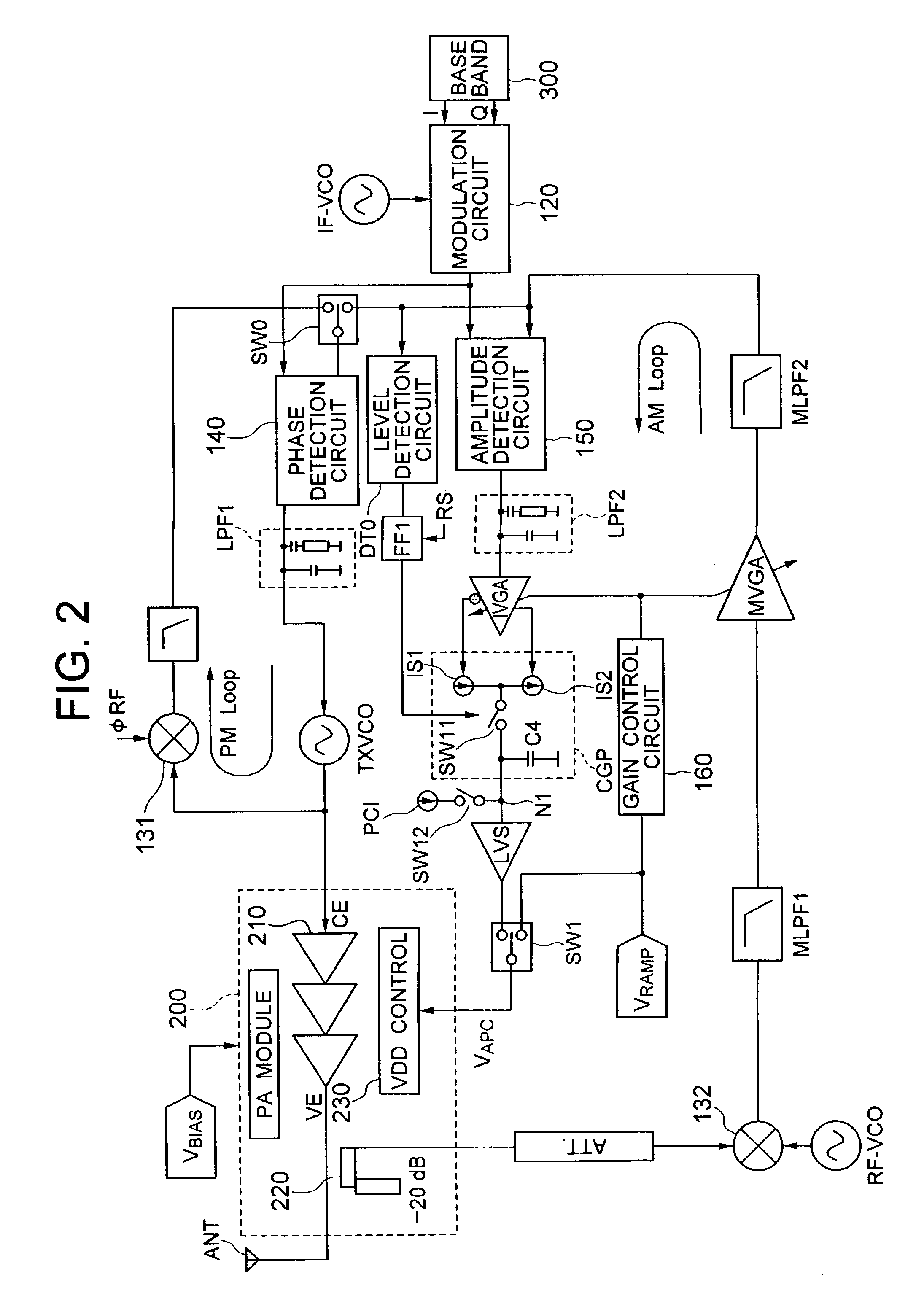
[0056]The precharge circuit in the second embodiment comprises a timer TMR for controlling the precharge current source PCI in addition to the like circuit in the first embodiment. The timer TMR can be configured to measure the time in response to a clock signal supplied from the baseband LSI 300. Also, the timer TMR may be provided integrally with other timers within the sequencer 180. The timer TMR is started simultaneously with the start of precharge at step S4 in FIG. 3, and the precharge current source PCI is turned off, for example, after the lapse of 5 μsec. In this way, the precharge can be terminated even if no change is found in the output of the level detection circuit DTC because the feedback signal has not reached the predetermined level at that time.
[0057]Even if constants of elements constituting the precharge circuit are set by design such that the output of the level shift circuit LVS, i.e., the output control voltage (VA...
third embodiment
[0062]FIG. 7 illustrates the precharge circuit.
[0063]The third embodiment applies a two-stage precharge method for precharging in stages the capacitor C4 which forms part of the charge pump CGP. Specifically, a switch SW13 is provided between a regulated voltage source CV1 (0.1 V) which provides a voltage as a reference for a shift amount (−0.6 V on the output side) in the level shift circuit LVS, and the node Ni to which the capacitor C4 is connected, such that the regulated voltage source CV1 can be utilized as a precharge power supply. In addition, the precharge current source PCI used herein supplies a smaller current value than the precharge current sources PCI in the first and second embodiments. Then, in the third embodiment, as illustrated in FIG. 8, the switch SW13 is first turned on within a short time T1 immediately after the output power is build up to precharge the capacitor C4 to 0.1 V by the regulated voltage source CV1. Subsequently, the switch SW12 is turned on to s...
PUM
 Abstract
Description
Claims
Application Information


