Activation signal output circuit and determination circuit

a signal output circuit and output circuit technology, applied in the direction of electronic switching, pulse technique, instruments, etc., can solve the problems of difficult suppression of power consumption during standby time difficult to achieve target lower power consumption, etc., to enhance detection sensitivity, sharply reduce erroneous detection, and enhance performance

Inactive Publication Date: 2007-04-24
DENSO CORP
View PDF19 Cites 8 Cited by
  • Summary
  • Abstract
  • Description
  • Claims
  • Application Information

AI Technical Summary

Benefits of technology

[0036]Further, the eighth invention of the present application resides in, in any of the first through seventh inventions, a matching circuit, which is connected to the first terminal side of the sensing diode Q1 to which the radio frequency power is inputted, for efficiently inputting the radio frequency power.
[0079]Further, according to the twenty-first invention of the present application, the low-pass filtering and amplification are attained only in the vicinity of the direct current with respect to frequency values. The other noises can therefore be effectively eliminated, so that a sensitivity can be enhanced much more than in the prior art diode wave detection.

Problems solved by technology

Under the premise of a battery operation or the like, however, lowering power consumption as desired is difficult when the operational amplifier requiring the current of mA order is adopted.
In such an apparatus, however, a signal generator, a LNA, a mixer, etc. must be always operated, and power consumption during a standby time period is therefore difficult to be suppressed.
Thus, the target lower power consumption is not attained, either.
On the other hand, the prior art sensing scheme based on the diode is difficult to enhance a sensing sensitivity.
These circumstances will be major causes for making difficult the compatibility between the higher sensitivity and lower power consumption of the wave-detector circuit.
As a result, the biases of the sensing diode and amplifier cannot be made independent.
On this occasion, however, unless the bias of the amplifier properly lowers in balanced fashion likewise to the bias of the diode detection circuit, the start signal output circuit 900 does not appropriately operate as a whole when the supply voltage Vcc lowers greatly.
That is, the circuit of the prior art arrangement (example: start signal output circuit 900 in FIG. 38), which does not have a flexible corresponding mechanism (balancing function) capable of coping with such a problem relevant to the lowering of the output voltage of the power supply, is apprehended to erroneously operate in some cases.
Further, in a high-temperature environment, thermal noise, flicker noise, etc. are liable to develop within a circuit as is often observed in case of using, for example, MOSFETs for the circuit.
As also seen from the foregoing circuit arrangement in FIG. 39B, the addition of such a determination circuit leads to increase of power consumption.
That is, it is not easy to operate the desired start signal output circuit as a whole, always at a low voltage and at a low current.
However, when an apparatus configuration in which also the peripheral devices must be always operated is adopted, the start signal output circuit of very low power consumption cannot be eventually constructed as the whole apparatus.
Moreover, such a problem becomes an issue or is actualized especially in cases of battery drive, etc.
When the high resistance of about several MΩ is formed on an IC chip as shown in FIG. 37 by way of example, the resistance element becomes long, and hence, a large space is necessitated.
Thus, a parasitic capacitance and a parasitic resistance appear between the resistance on the chip and the ground within a substrate, and radio frequency power leaks to the substrate.
Further, as other problems concerning the diode wave detection, it is pointed out that, in a case where the load resistance becomes high, the applied voltage between the anode and cathode of the diode becomes small, so radio frequency power cannot be converted into a direct current, and that, even in a case where the radio frequency power is successfully converted into the direct current, it is indistinguishable whether the output potential fluctuation of the diode is ascribable to the fluctuation of a bias or the DC conversion of the RF power.
However, each object mentioned above may be individually accomplished by any and at least one of inventions to be described later, and the individual inventions of the present application shall not necessarily guarantee that means capable of simultaneously solving all the above problems be existent.

Method used


Image

  • Activation signal output circuit and determination circuit
  • Activation signal output circuit and determination circuit
  • Activation signal output circuit and determination circuit

Examples


second embodiment

(Second Embodiment)

[0188]The second embodiment exemplified in conjunction with the drawings of FIGS. 13 through 24 is in order to solve these problems. As means for solving the problems, by way of example, the foregoing embodiment is modified so that a voltage doubler wave-detector circuit can be utilized for the detection / amplification circuit, an S / N ratio is enhanced by employing MOSFETs of large gates, or it is permitted to obtain a large amplitude by introducing active loads configured of transistors, into the determination circuit. Further, a combination with a binarization circuit utilizing CMOS is considered so that the power consumption can be further lowered.

[Voltage Doubler Wave-Detector Circuit]

[0189]FIG. 13 is a circuit diagram exemplifying a start signal output circuit 200 in the second embodiment. Further, FIG. 14 is a circuit diagram of a detection / amplification circuit 210 which is included in the start signal output circuit 200. In the second embodiment, first of a...

third embodiment

(Third Embodiment)

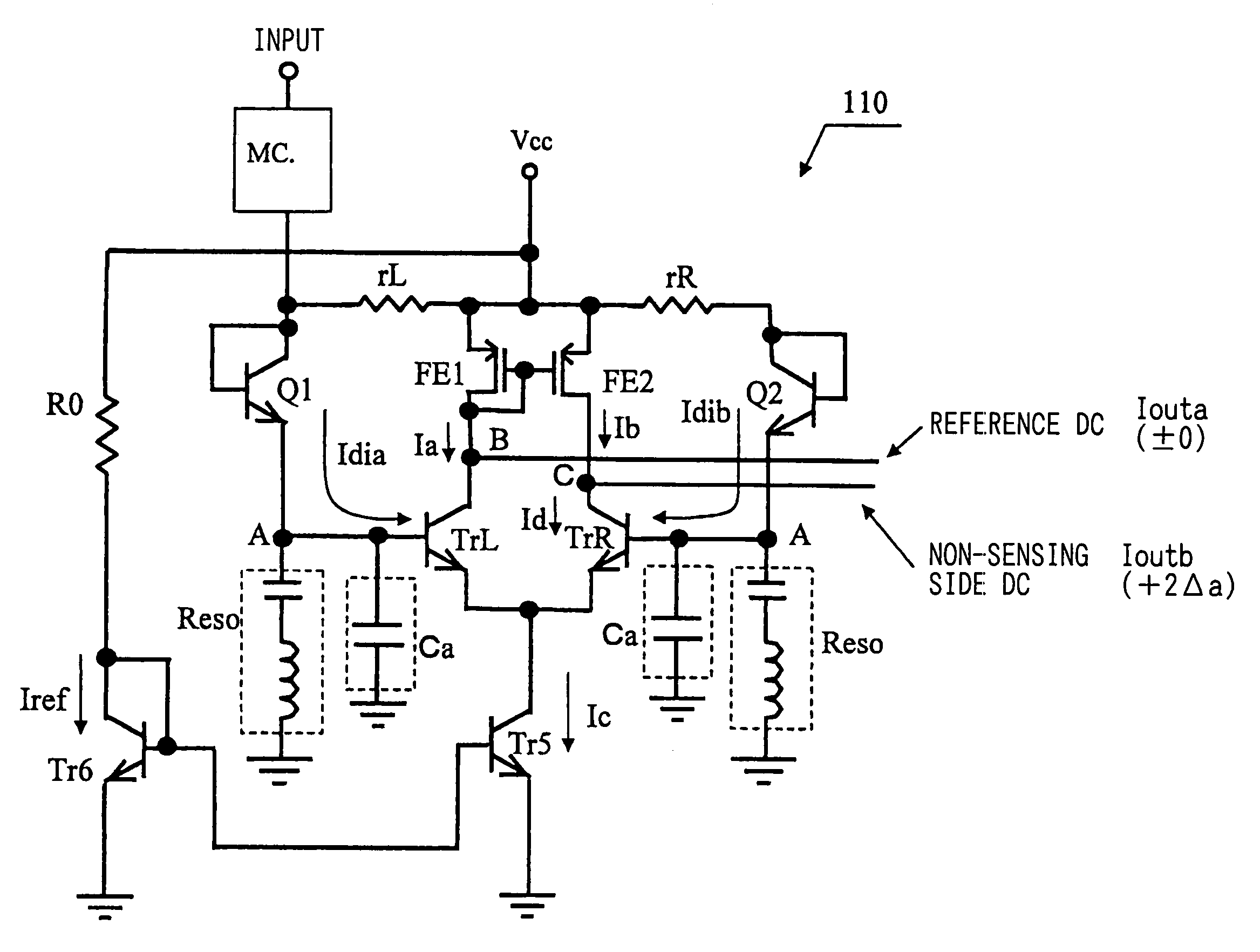
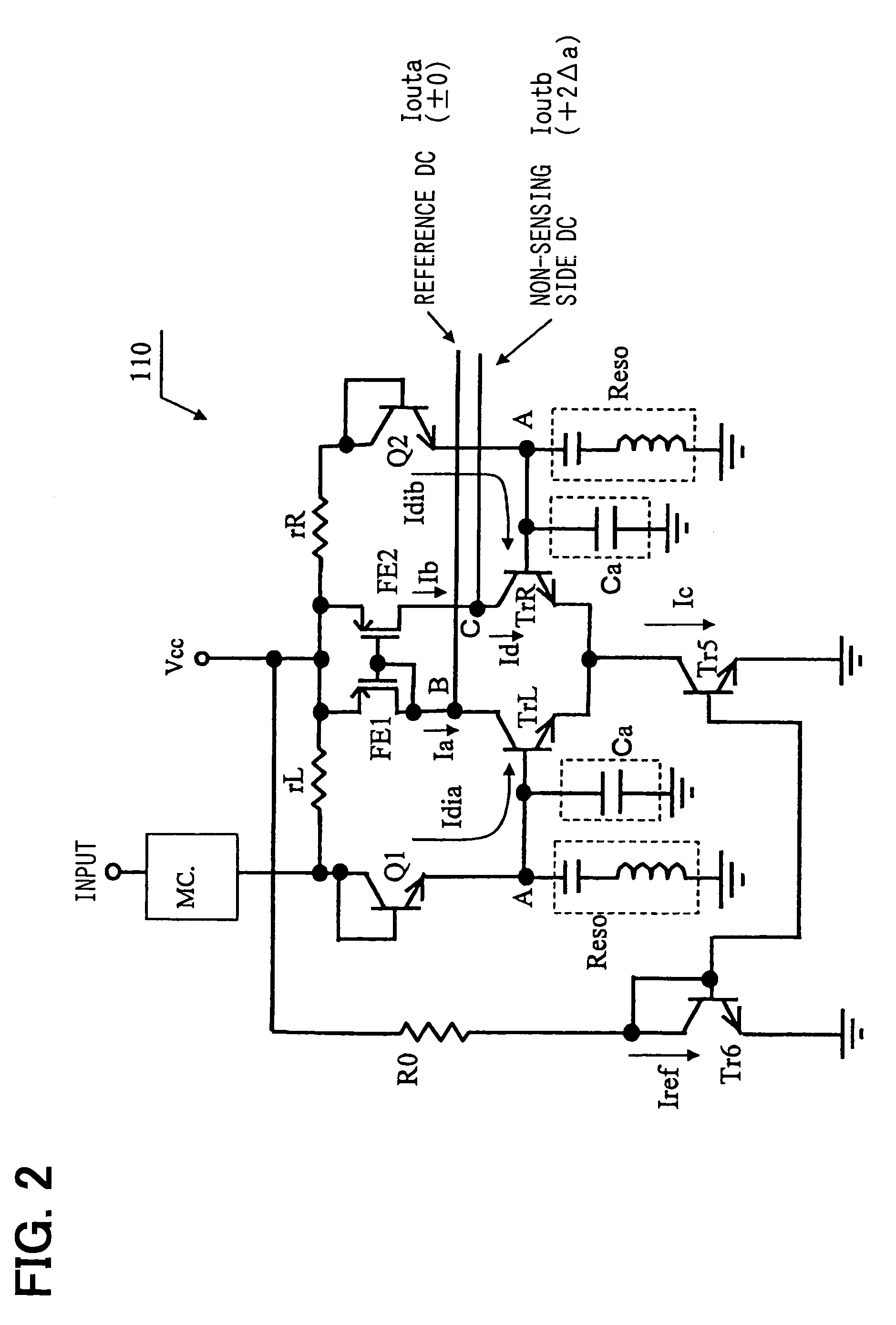
[0227]As a method for attaining a large amplitude (gain) in the determination circuit (example: determination circuit 120 in FIG. 1), there is described, for example, the method in which the appropriate load resistors (ra, rb and rc) are employed as exemplified in detail in FIG. 3 in the foregoing first embodiment. Alternatively, however, there is a method in which the gain of the differential pair transistors of the differential amplifier of the determination circuit is enhanced. The method is, for example, one in which Darlington connection is employed for the part of the differential pair transistors of the differential amplifier of the determination circuit.

[0228]FIG. 25 exemplifies a determination circuit 222 in which the determination circuit 120 (FIG. 3) in the foregoing first embodiment is reconfigured using the Darlington connection. Incidentally, also here, load resistors are set at Ra

fourth embodiment

(Fourth Embodiment)

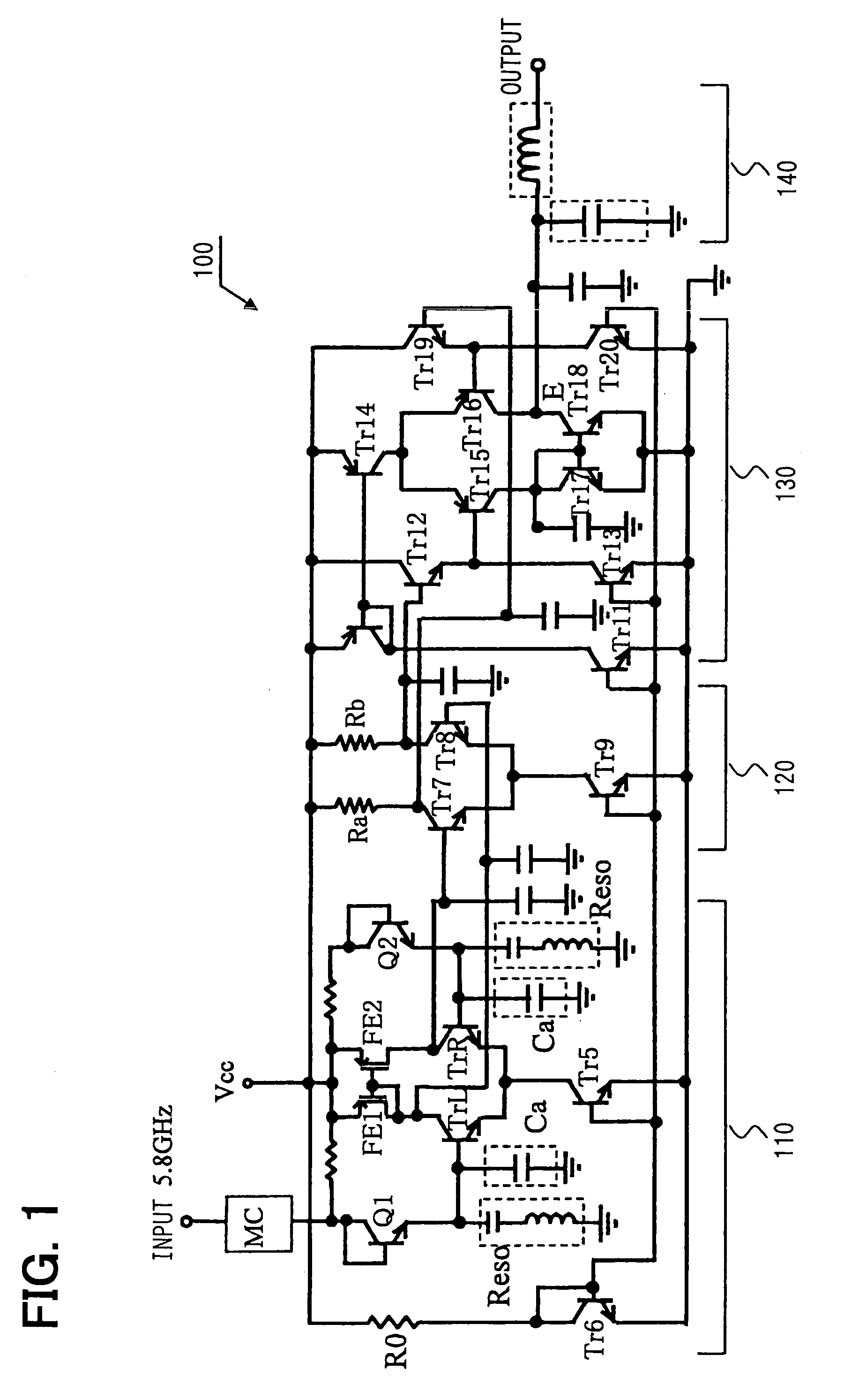
[0236]Shown in FIG. 30 is a circuit diagram of a start signal output circuit 201 in the fourth embodiment as is provided in such a way that, in the start signal output circuit 200 of the second embodiment, the binarization circuit 230 is replaced with the binarization circuit 130 in the first embodiment.

[0237]More specifically, here, the wave-detector circuit of voltage doubler form (voltage doubler wave-detector circuit) in FIG. 16B is employed as a detection / amplification circuit 210, and the active loads (FIGS. 17 and 18) constructed using the bipolar transistors Tr23 and Tr24 are adopted for the loads of the determination circuit 220. However, the output form of the determination circuit 220 is a two-output form, and regarding a low pass filter 140 further disposed at the succeeding stage of the binarization circuit 130, one of the same form as in the foregoing first embodiment (FIG. 1) is employed.

[0238]Here, signs in the figure in the fourth embodiment are a...


PUM


Abstract

A start signal output circuit having an RF / DC conversion circuit to which radio frequency power (RF) of specified frequency is inputted and from which a direct current potential (DC) is outputted, comprises a detection / amplification circuit 210 which includes a voltage doubler wave-detector circuit 10 configured including a sensing diode Q1 (Tr34) for sensing the RF power, a differential amplifier including differential pair transistors Tr31 and Tr32, and a current mirror circuit. A base current of one Tr31 of the differential pair transistors is brought into substantial agreement with a DC component of a current flowing through the sensing diode Q1 (Tr34). A total of currents flowing through the differential pair transistors Tr31 and Tr32 is regulated to a substantially constant value by the current mirror circuit. Thus, the start signal output circuit which is small in size, high in sensitivity and low in power consumption can be realized.

Description

TECHNICAL FIELD[0001]The present invention relates to a start signal output circuit having an RF / DC conversion circuit, which inputs radio frequency power (RF) of specified frequency and outputs direct current potential (DC), and a determination circuit very useful for the start signal output circuit and the like.[0002]Herein, the direct current potential (DC) signifies an output potential which is generated on the basis of a detection potential from a sensing diode as developing during a time period for which the level (amplitude) of a waveform determined by the envelope of the waveform of the radio frequency power (RF) has a substantially constant value or above.[0003]Accordingly, in a case where the RF power arrives intermittently or where the arrival is periodic, the waveform of the DC potential can become periodic. Even in a case, for example, where the DC potential fluctuates periodically or intermittently in such a manner, the present invention is, of course, useful.[0004]Tha...

Claims


Application Information

Patent Timeline
Patent Type & Authority Patents(United States)
IPC IPC(8): G06F19/00H03F3/45H03D1/10H03D1/18H03F3/68
CPCH03D1/10H03D1/18
Inventor MIZUNO, KAZUOKIMURA, RYUKAGO, YOSHIYUKITANAKA, YUKIOMIENDO, KAZUHIKOUDA, HISANORIHAYASHI, HIROAKI
Owner DENSO CORP
Why Eureka
Try Eureka