

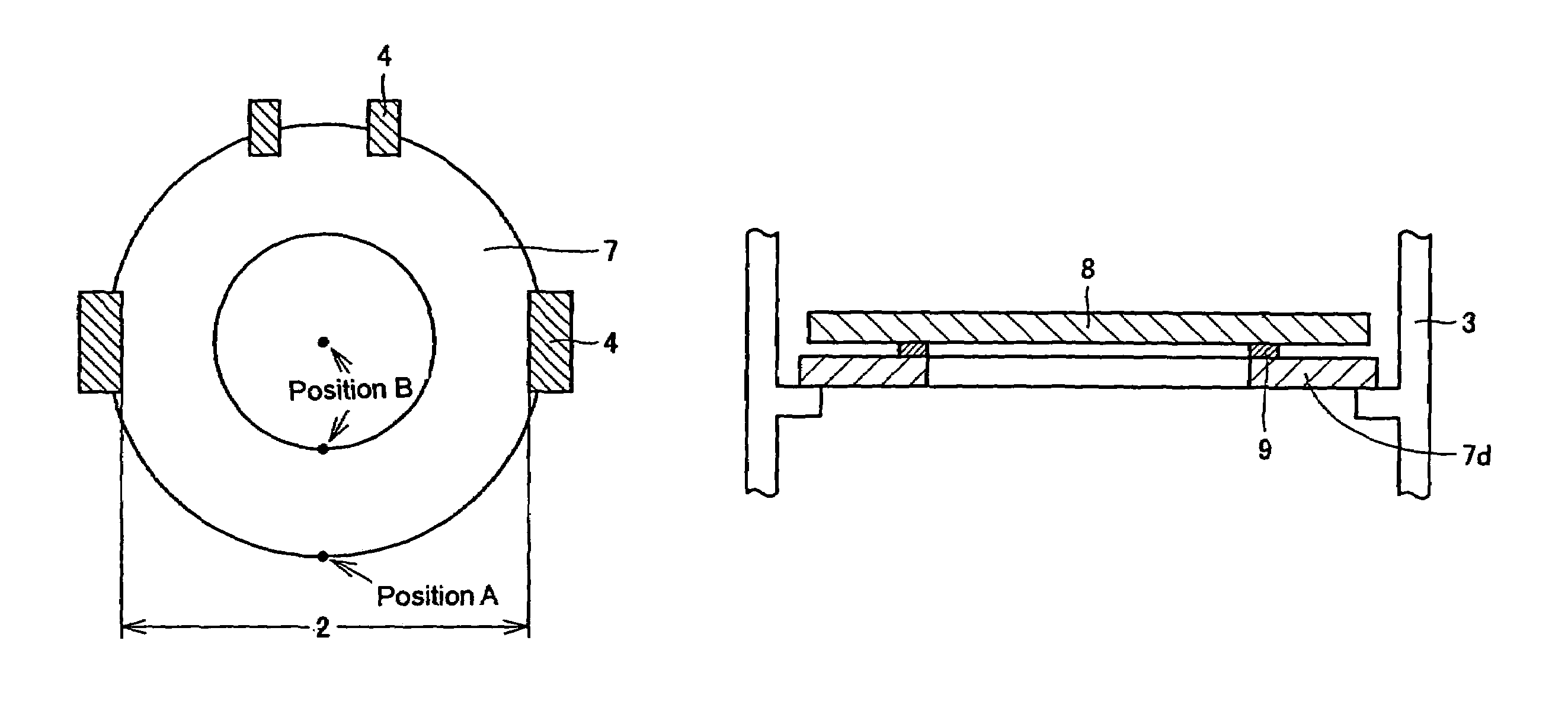
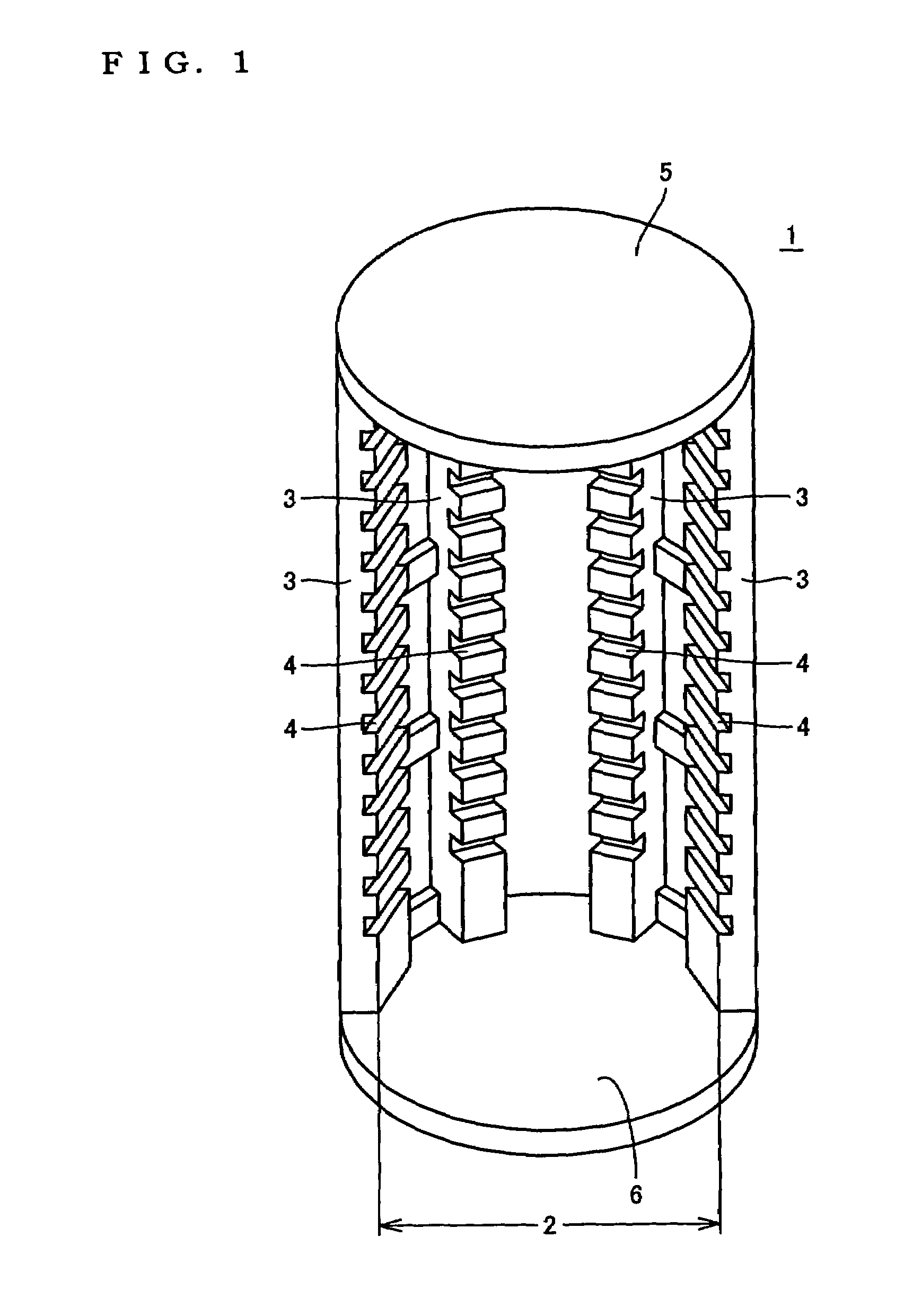
Heat treatment jig for silicon semiconductor substrate
a silicon semiconductor substrate and heat treatment technology, applied in the direction of charging supports, lighting and heating apparatus, furniture, etc., can solve the problems of thermally oxidized film being hindered, the thickness of the jig is thinner, and the heat treatment jig to date cannot fully meet the requirement of preventing the generation of slips, so as to reduce the surface steps, reduce the effect of slip generation, and reduce the thickness
- Summary
- Abstract
- Description
- Claims
- Application Information
AI Technical Summary
Benefits of technology
Problems solved by technology
Method used
Image

Examples
example 1
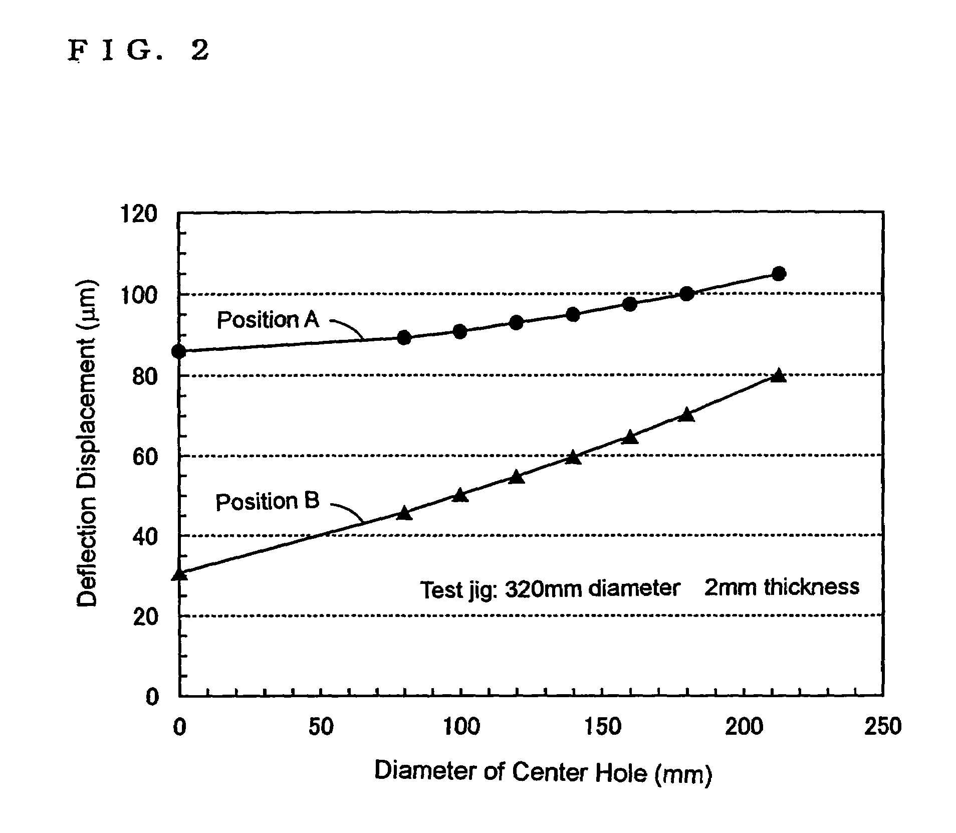
[0078]For confirmatory purpose of the proper wall thickness of the jig, three jigs each having a solid disc structure made of silicon carbide (SiC) were prepared as for the jigs of Inventive example No. 1, wherein the detail is set as follows; the diameter of 319 mm; the wall thickness of 1.5 mm; the amount of generated deflection displacement of 40 μm to 60 μm; and the surface roughness of 1.5 μm to 1.7 μm.
[0079]Similarly, as for the jigs of Comparative example No. 1, three jigs each having a solid disc structure made of silicon carbide (SiC) were prepared, wherein the detail parameter is set as follows; the diameter of 319 mm; the wall thickness of 0.9 mm; the amount of generated deflection displacement of 50 μm to 80 μm; and the surface roughness of 1.4 μm to 1.7 μm.
[0080]Silicon substrates of 300 mm diameter were charged onto these heat treatment jigs and heat treated in argon gas atmosphere in a vertical heat treatment furnace with the pattern as follows; heat-up rate of 5° C. / ...
example 2
[0083]As the jigs of Inventive example No. 2, fifty (50) jigs each having a solid disc structure made of SiC were prepared, wherein the detail parameter is set as follows; the diameter of 319 mm; the wall thickness of 2.0 mm; the amount of the generated deflection displacement of 30 μm to 60 μm; and the surface roughness of 1.5 μm to 2.0 μm.
[0084]The prepared jigs of Inventive example No. 2 were loaded onto the vertical heat treatment boat with a pitch of 12 mm and were heat treated exactly in the same manner with Example 1. After the heat treatment, silicon substrates were examined for the slip by using a mirror magic apparatus, observing that the slips were generated at the peripheral portions for almost all silicon substrates.
[0085]Next, the same jigs of Inventive example No. 2 were loaded onto the vertical heat treatment boat with a pitch of 12 mm and were heat treated in similar manner to Example 1 except that the heating and cooling rate in the range from 1000° C. to 1200° C. ...
example 3
[0088]Further, by utilizing the remaining jigs that through-wall holes were disposed in above Example 2, the jigs of Inventive example Nos. 4 through 6 were prepared.
[0089]First, as the jigs of Inventive example No. 4, ten (10) jigs each having a solid disc structure made of SiC were prepared, wherein the detail parameter is set as follows; the diameter of 210 mm; the wall thickness of 1.8 mm; the amount of the generated deflection displacement of 30 μm to 60 μm; and the surface roughness of 2.1 μm to 2.3 μm.
[0090]Next, as the jigs of Inventive example No. 5, ten (10) jigs each having a ring structure made of SiC were prepared, wherein the detail parameter is set as follows; the diameter of 210 mm; the inside diameter of 205 mm; the wall thickness of 1.8 mm; the amount of the generated deflection displacement of 30 μm to 60 μm; and the surface roughness of 2.1 μm to 2.2 μm.
[0091]Further, as the jigs of Inventive example No. 6, ten (10) jigs each having a ring structure made of SiC w...
PUM
 Abstract
Description
Claims
Application Information