Supercharge Your Innovation With Domain-Expert AI Agents!

Methods of forming silicon dioxide layers, and methods of forming trench isolation regions

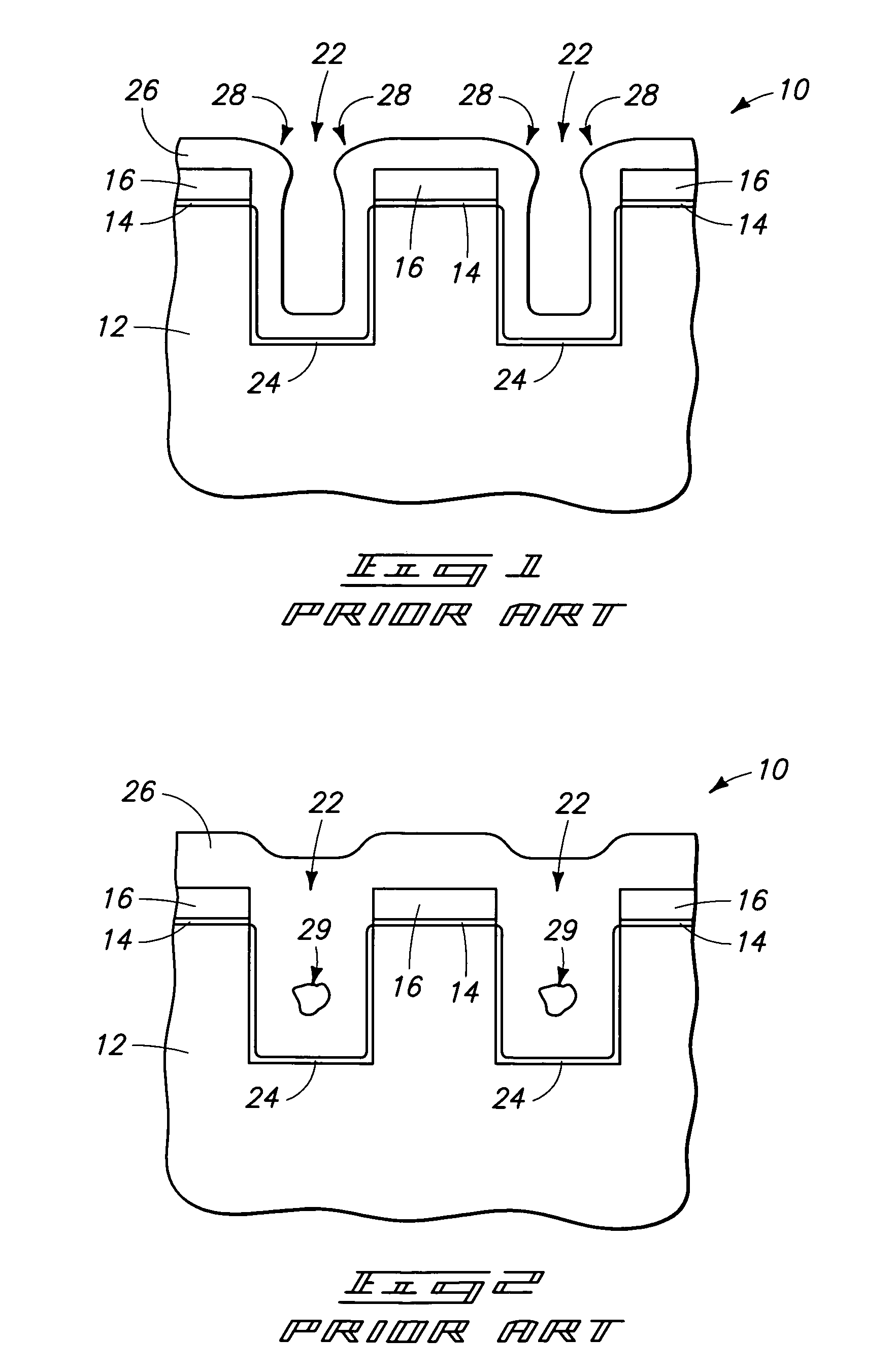
a technology of silicon dioxide and trench isolation, applied in the direction of coatings, chemical vapor deposition coatings, metallic material coating processes, etc., can solve the problem of undesirable current leakage through the trench isolation region

Inactive Publication Date: 2007-05-01
MICRON TECH INC
View PDF47 Cites 0 Cited by
  • Summary
  • Abstract
  • Description
  • Claims
  • Application Information

AI Technical Summary

Benefits of technology

This approach ensures a conformal coating with improved step coverage and eliminates voids in trench isolation regions, reducing current leakage and enhancing the quality of silicon dioxide layers.

Problems solved by technology

The voids define a space within the trench isolation regions having a different dielectric constant than the remainder of the trench isolation regions, and can undesirably allow current leakage through the trench isolation regions.

Method used


Image

  • Methods of forming silicon dioxide layers, and methods of forming trench isolation regions
  • Methods of forming silicon dioxide layers, and methods of forming trench isolation regions
  • Methods of forming silicon dioxide layers, and methods of forming trench isolation regions

Examples


Embodiment Construction

[0020]This disclosure of the invention is submitted in furtherance of the constitutional purposes of the U.S. Patent Laws “to promote the progress of science and useful arts” (Article 1, Section 8).

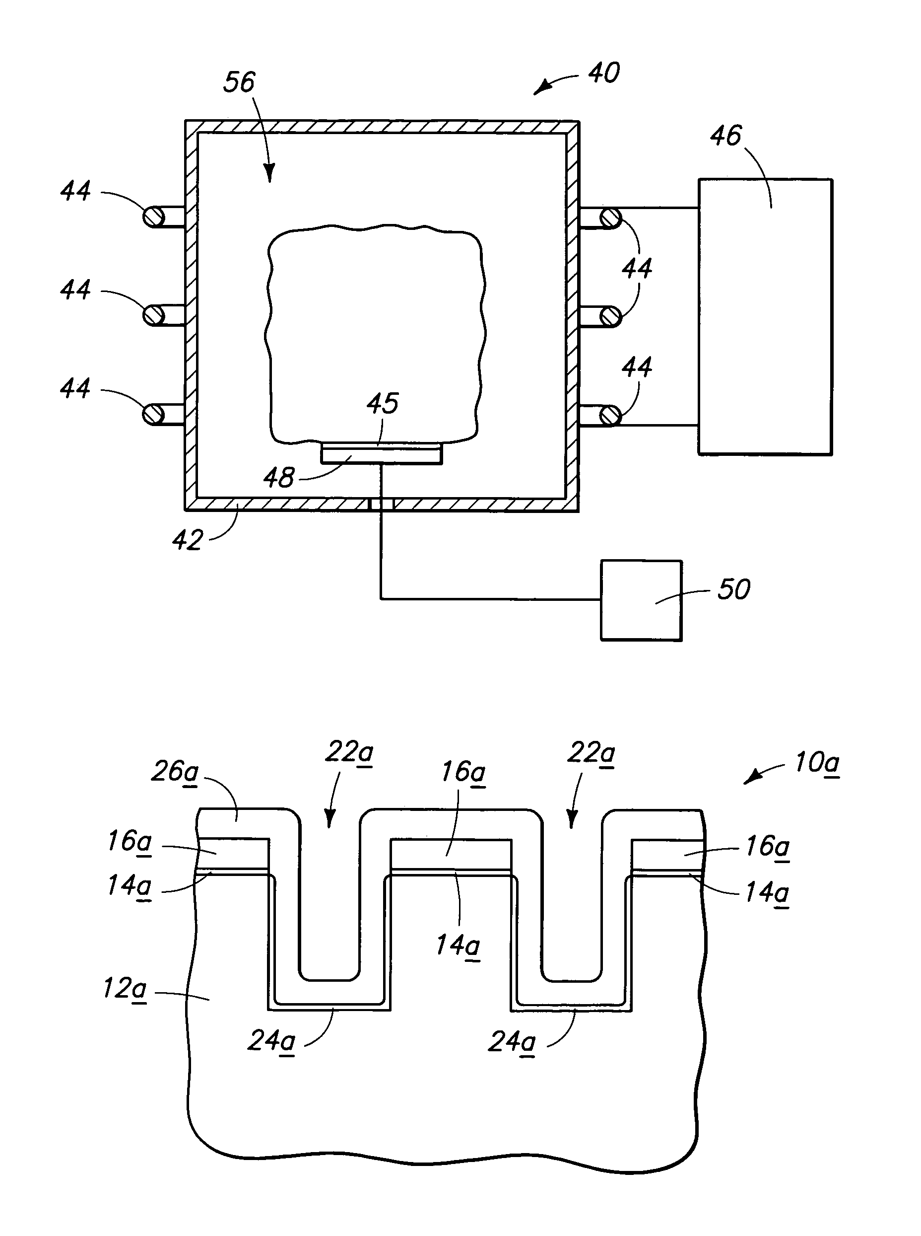
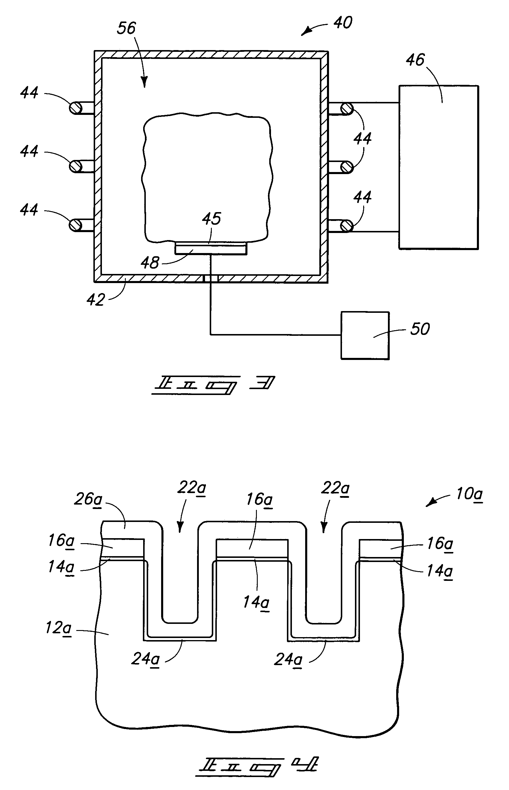
[0021]The present invention encompasses methods of increasing a deposition to etch ratio in a high density plasma reaction chamber during formation of a silicon dioxide layer. A high density plasma reaction chamber 40 is illustrated in FIG. 3. Reaction chamber 40 comprises a vessel 42 surrounded by inductive coils 44. Inductive coils 44 are connected to a first power source 46 which can be configured to provide power, such as, for example, RF energy, within coils 44. Reaction chamber 40 further comprises a chuck 48 configured for holding a semiconductive wafer 45 within vessel 42. Wafer 45 is connected through chuck 48 to a power source 50 which can be configured to, for example, produce RF energy within wafer 45.

[0022]In operation, plasma precursor gasses (not shown) are flowed into vess...


PUM

PropertyMeasurementUnit
distanceaaaaaaaaaa
temperatureaaaaaaaaaa
poweraaaaaaaaaa

Abstract

A method of forming a silicon dioxide layer includes forming a high density plasma proximate a substrate, the plasma comprising silicon dioxide precursors; forming silicon dioxide from the precursors, the silicon dioxide being deposited over the substrate at a deposition rate; and while depositing, etching the deposited silicon dioxide with the plasma at an etch rate; a ratio of the deposition rate to the etch rate being at least about 4:1. Another method includes forming a high density plasma proximate a substrate; flowing gases into the plasma, at least some of the gases forming silicon dioxide; depositing the silicon dioxide formed from the gases over the substrate; and while depositing the silicon dioxide, maintaining a temperature of the substrate at greater than or equal to about 500° C. As an alternative, the method may include not cooling the substrate with a coolant gas while depositing the silicon dioxide.

Description

RELATED PATENT DATA[0001]This patent resulted from a continuation of U.S. patent application Ser. No. 10 / 815,065, filed Mar. 30, 2004, now U.S. Pat. No. 7,018,908, which is a continuation of U.S. patent application Ser. No. 09 / 497,080, filed on Feb. 2, 2000, now U.S. Pat. No. 6,737,328, which resulted from a divisional application of U.S. patent application Ser. No. 09 / 113,467, filed on Jul. 10, 1998, now U.S. Pat. No. 6,759,306, the subject matter of which are herein incorporated by reference.TECHNICAL FIELD[0002]The invention pertains to methods of forming silicon dioxide layers, such as, for example, methods of forming trench isolation regions.BACKGROUND OF THE INVENTION[0003]Integrated circuitry is typically fabricated on and within semiconductor substrates, such as bulk monocrystalline silicon wafers. In the context of this document, the term “semiconductive substrate” is defined to mean any construction comprising semiconductive material, including, but not limited to, bulk se...

Claims


Application Information

Patent Timeline
Patent Type & Authority Patents(United States)
IPC IPC(8): H01L21/76H01L21/316H01L21/762
CPCC23C16/045C23C16/402H01L21/02164H01L21/02211H01L21/02274H01L21/31612H01L21/76224H01L21/76
Inventor SHARAN, SUJITSANDHU, GURTEJ S.
Owner MICRON TECH INC
Features
  • R&D
  • Intellectual Property
  • Life Sciences
  • Materials
  • Tech Scout
  • Unparalleled Data Quality
  • Higher Quality Content
  • 60% Fewer Hallucinations
Learn More