Method of forming insulating layer in semiconductor device

a technology of insulating film and semiconductor device, which is applied in the direction of coating, nanotechnology, chemical vapor deposition coating, etc., can solve the problems of difficult to control the fine structure of the film, the dielectric constant of the semiconductor device is difficult to be below 2.7, and the operating speed of the parasitic capacitor is degraded

Inactive Publication Date: 2007-05-01
SK HYNIX INC
View PDF11 Cites 356 Cited by
  • Summary
  • Abstract
  • Description
  • Claims
  • Application Information

AI Technical Summary

Benefits of technology

[0007]The present invention is contrived to solve the above problems and an object of the present invention is to provide a method of forming an insulating film in a semiconductor device by which a low-dielectric insulating film that can be applied to the nano technology can be formed even using the existing deposition equipment. To this end, af...

Problems solved by technology

With this structure, the parasitic capacitor is formed and the parasitic capacitor degrades the operating speed of the device.
However, if the concentration of hydrocarbon is increased, it is difficult to lower the dielectric constant below 2.7 since thermal stability and mechanical st...

Method used


Image

  • Method of forming insulating layer in semiconductor device
  • Method of forming insulating layer in semiconductor device
  • Method of forming insulating layer in semiconductor device

Examples


Embodiment Construction

[0017]The present invention will be described in detail by way of a preferred embodiment with reference to accompanying drawings.

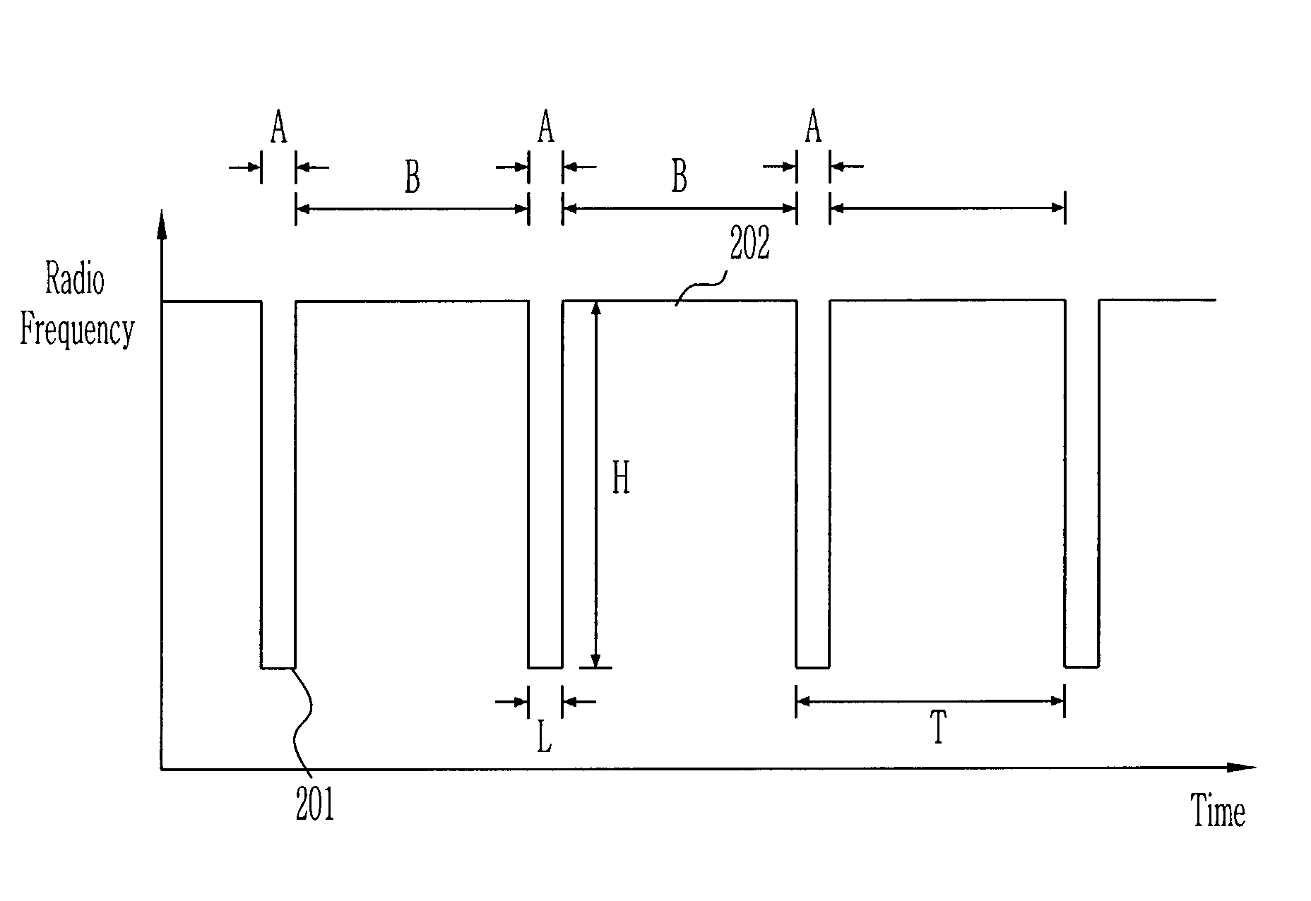
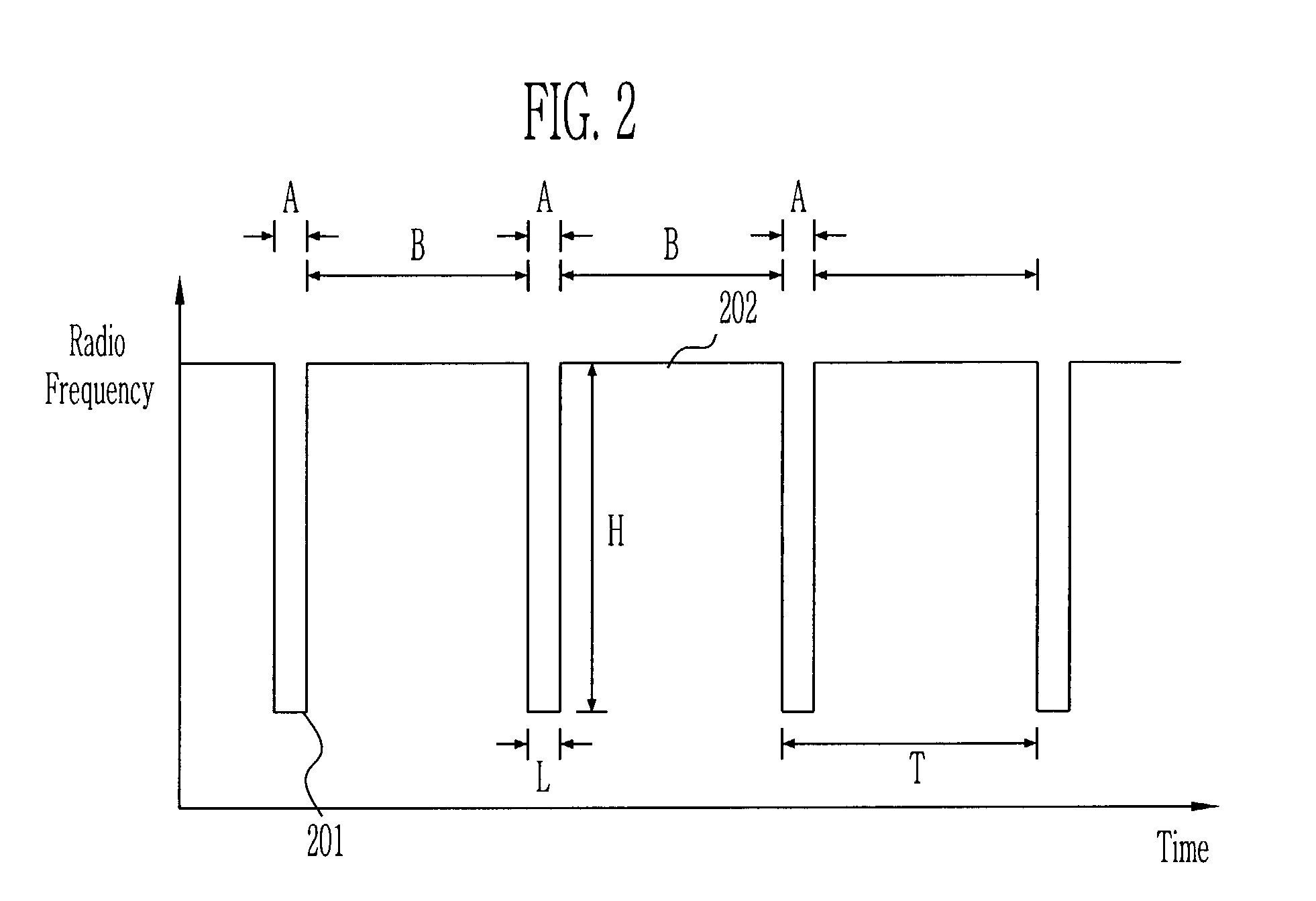
[0018]FIG. 1A and FIG. 1B are cross-sectional views of semiconductor devices for explaining a method of forming an insulating film in the semiconductor device according to a preferred embodiment of the present invention, and FIG. 2 is a graph illustrating a waveform of the radio frequency power applied during the process of forming the insulating film.

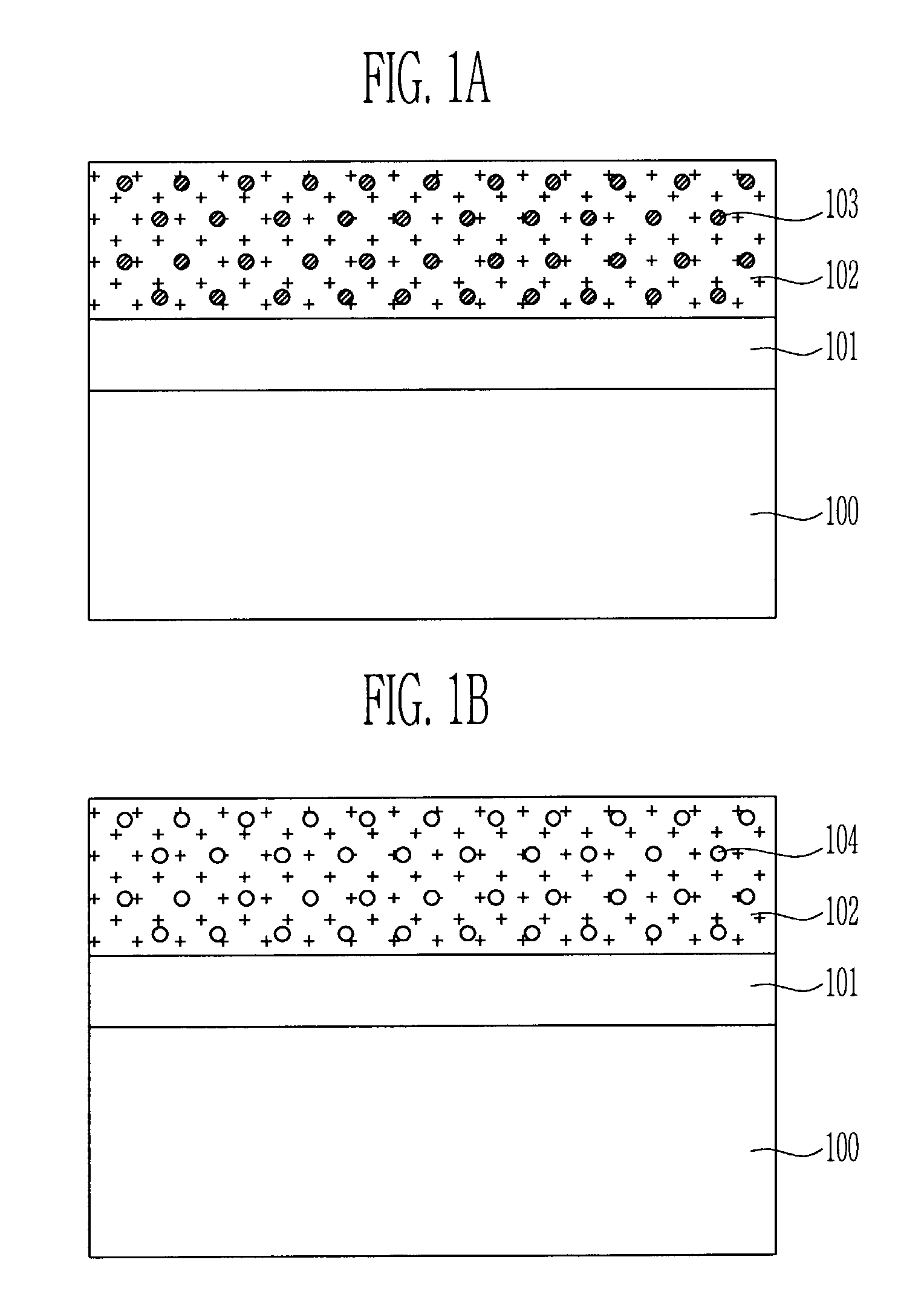
[0019]Referring now to FIG. 1A, a semiconductor substrate 100 in which a lower structure 101 such as a transistor, a metal line, a capacitor and a memory cell is formed is mounted on the deposition equipment (not shown).

[0020]After the semiconductor substrate 100 is mounted, insert gas such as He or Ar is supplied into the deposition equipment to control the reaction pressure. At this time, it is preferred that the inert gas is supplied at a flow rate of 500 through 5000 sccm and an internal pressure of the d...


PUM

PropertyMeasurementUnit
Poweraaaaaaaaaa
Poweraaaaaaaaaa
Flow rateaaaaaaaaaa

Abstract

The present invention relates to a method of forming an insulating film in a semiconductor device. After a mixed gas of alkyl silane gas and N2O gas is supplied into the deposition equipment, a radio frequency power including a short pulse wave for causing incomplete reaction upon a gas phase reaction is applied to generate nano particle. The nano particle is then reacted to oxygen radical to form the insulating film including a plurality of nano voids. A low-dielectric insulating film that can be applied to the nano technology even in the existing LECVD equipment is formed.

Description

BACKGROUND OF THE INVENTION[0001]1. Field of the Invention[0002]The invention relates generally to a method of forming an insulating film in a semiconductor device. More particularly, the invention relates to a method of forming an insulating film in a semiconductor device by which a low-dielectric insulating film that will be applied to the nano technology in the deposition equipment including the existing PECVD (plasma enhanced chemical vapor deposition) equipment.[0003]2. Description of the Prior Art[0004]As the level of integration in the semiconductor device is increased, a metal line is formed in multiple layers. In order to electrically insulate these lines, an inter-metal line insulating film is formed between the metal line layers. The dielectric constant of the inter-metal line insulating film is changed depending on the type of materials. The performance of the device is dependent on the dielectric constant. In other words, the inter-line insulating film is formed between...

Claims


Application Information

Patent Timeline
IPC IPC(8): H01L21/31H01L21/469H01L21/205C23C16/40C23C16/515C23C16/56H01L21/316
CPCC23C16/401C23C16/515C23C16/56H01L21/02126H01L21/02203H01L21/02211H01L21/02274H01L21/0228H01L21/31633H01L21/31695B82Y40/00
Inventor RYU, CHOON KUNKIM, TAE KYUNG
Owner SK HYNIX INC
Why Eureka
Try Eureka