

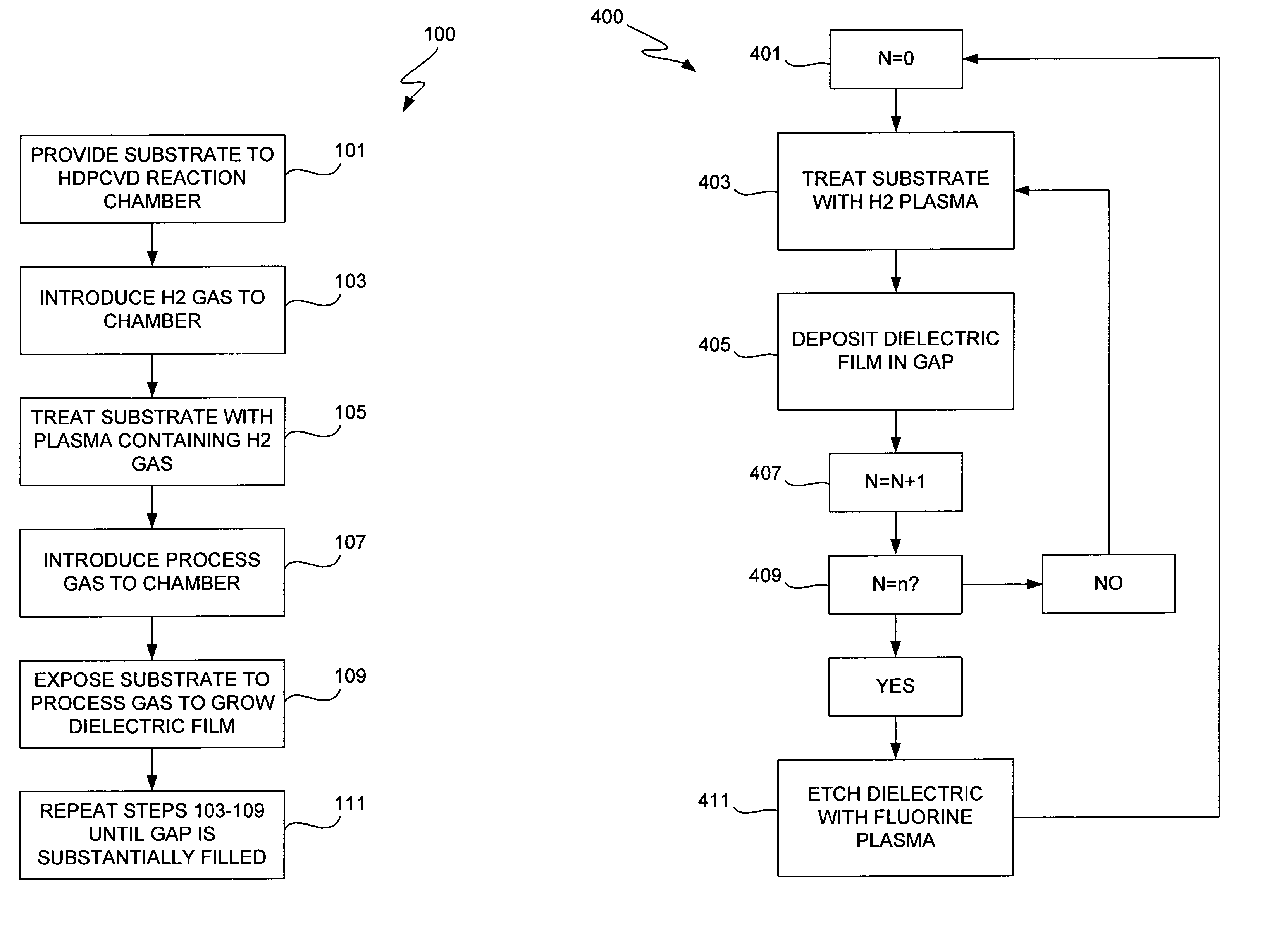
Hydrogen treatment enhanced gap fill
a technology of hydrogen treatment and enhanced gap filling, which is applied in the direction of coating, chemical vapor deposition coating, metallic material coating process, etc., can solve the problems of reducing budgets, increasing the difficulty of void-free filling of high aspect ratio spaces (e.g., ar>3:1), and sometimes closing the top part of high aspect ratio structures. , to reduce or eliminate sidewall deposition, reduce or eliminate the need for etch steps
- Summary
- Abstract
- Description
- Claims
- Application Information
AI Technical Summary
Benefits of technology
Problems solved by technology
Method used
Image

Examples
example 1
[0077]Dielectric film was deposited on bare (new and recycled) wafers and pre-deposited wafers containing a layer of at least 2000 Å of SiO2 film. The following process parameters were used:
[0078]
ParameterH2 TreatmentDepositionInjectionTwin injectionTwin injectionSilane flow rate, sccm040Oxygen flow rate, sccm065Helium flow rate, sccm0250Hydrogen flow rate, sccm1800490NF3, sccm00LFRF (side coil), W25004500MFRF (top coil), W25004500HFRF (bias), W01800Pedestal - distance from1.53.75gas ring, inches
[0079]Deposition rates were found as functions of various hydrogen treatment times and deposition times (SDTs). The results are shown in FIG. 3 and discussed above. It should be noted that although pedestal distance from the gas ring was 1.5″, additional testing has shown that a pedestal distance of 3.75″ (i.e. the same used during deposition) also works well.
example 2
[0080]Dielectric film was deposited on treated and untreated 200 mm wafers using a SPEED-NExT chamber, available from Novellus Systems of San Jose, Calif. For both processes, SiH4 flow rate was 40 sccm and deposition rate was approximately 2200 Å / min.
[0081]For the untreated substrate, a thickness of 2000 Å deposited film was targeted. A single step deposition with an SDT of 57 seconds was used. No etch steps were used.
[0082]For the treated substrate, a thickness of 2500 Å deposited film was targeted. 5 cycles of 40 sccm SiH4 were used with an SDT of 14 seconds. No etch steps were used. H2 flow rate was 1500 sccm and treatment time was 10 seconds. The substrate was unbiased during treatment.
[0083]FIGS. 7A and 7B are rough schematic diagrams of the partially filled trenches after deposition; FIG. 7A shows the results obtained without hydrogen treatment and FIG. 7B with hydrogen treatment. The bottom thickness of the trench in FIG. 7A is less than that in FIG. 7B. In addition, FIG. 7A ...
example 3
[0087]Dielectric film was deposited on treated and untreated 200 mm wafers using a SPEED-NExT chamber, available from Novellus Systems of San Jose, Calif. For both processes, SiH4 flow rate was 80 sccm and deposition rate was approximately 4500 Å / min.
[0088]For the untreated substrate, a thickness of 2000 Å deposited film was targeted. A single step deposition with an SDT of 27 seconds was used. No etch steps were used.
[0089]For the treated substrate, a thickness of 2500 Å deposited film was targeted. 5 cycles of 80 sccm SiH4 were used with an SDT of 6 seconds. H2 flow rate was 1500 sccm and treatment time was 10 seconds. The substrate was unbiased during treatment. No etch steps were used.
[0090]FIGS. 8A and 8B are rough schematic diagrams of the partially filled trenches after deposition; FIG. 8A shows the results obtained without hydrogen treatment and FIG. 8B with hydrogen treatment. The bottom thickness of the trench in FIG. 8A is slightly less than that in FIG. 8B. In addition, ...
PUM
| Property | Measurement | Unit |
|---|---|---|
| time | aaaaa | aaaaa |
| time | aaaaa | aaaaa |
| time | aaaaa | aaaaa |
Abstract
Description
Claims
Application Information