
Organic electroluminescent display

a technology of electroluminescent display and organic material, which is applied in the direction of thermoelectric devices, identification means, instruments, etc., can solve the problems of contact failure, over-etching of the pad,

Active Publication Date: 2007-05-01
SAMSUNG DISPLAY CO LTD
View PDF18 Cites 26 Cited by
  • Summary
  • Abstract
  • Description
  • Claims
  • Application Information

AI Technical Summary

Benefits of technology

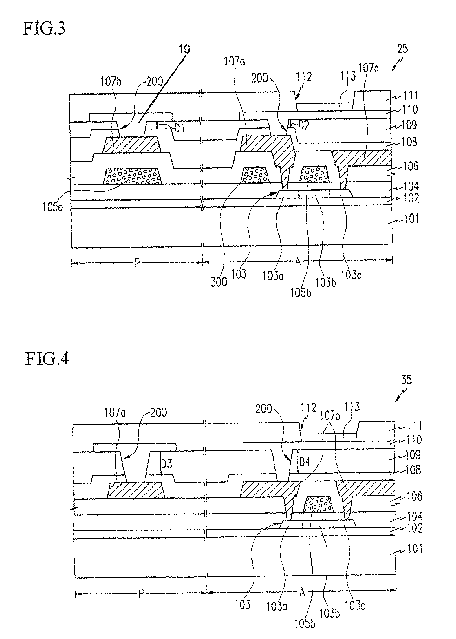
[0021]One of the aspects of the present invention is to prevent the source electrode and the drain electrode from being over-etched.
[0022]The present invention enables to reduce the thickness difference of the passivation layer between the array portion and the pad portion.

Problems solved by technology

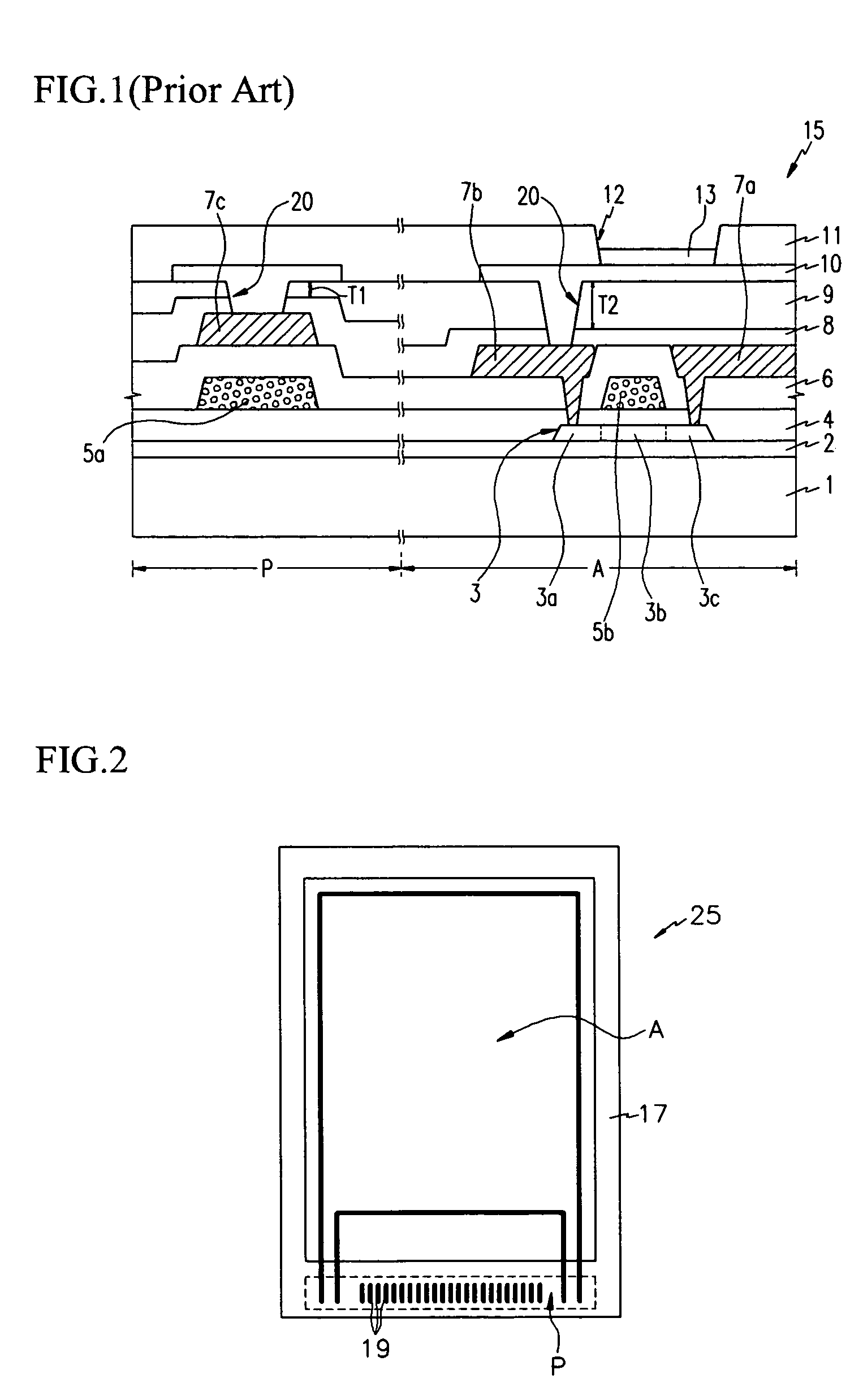
This results in over-etching of the pad 7c.
Then electrode over-etching causes contact failures.

Method used


Image

  • Organic electroluminescent display
  • Organic electroluminescent display
  • Organic electroluminescent display

Examples


Embodiment Construction

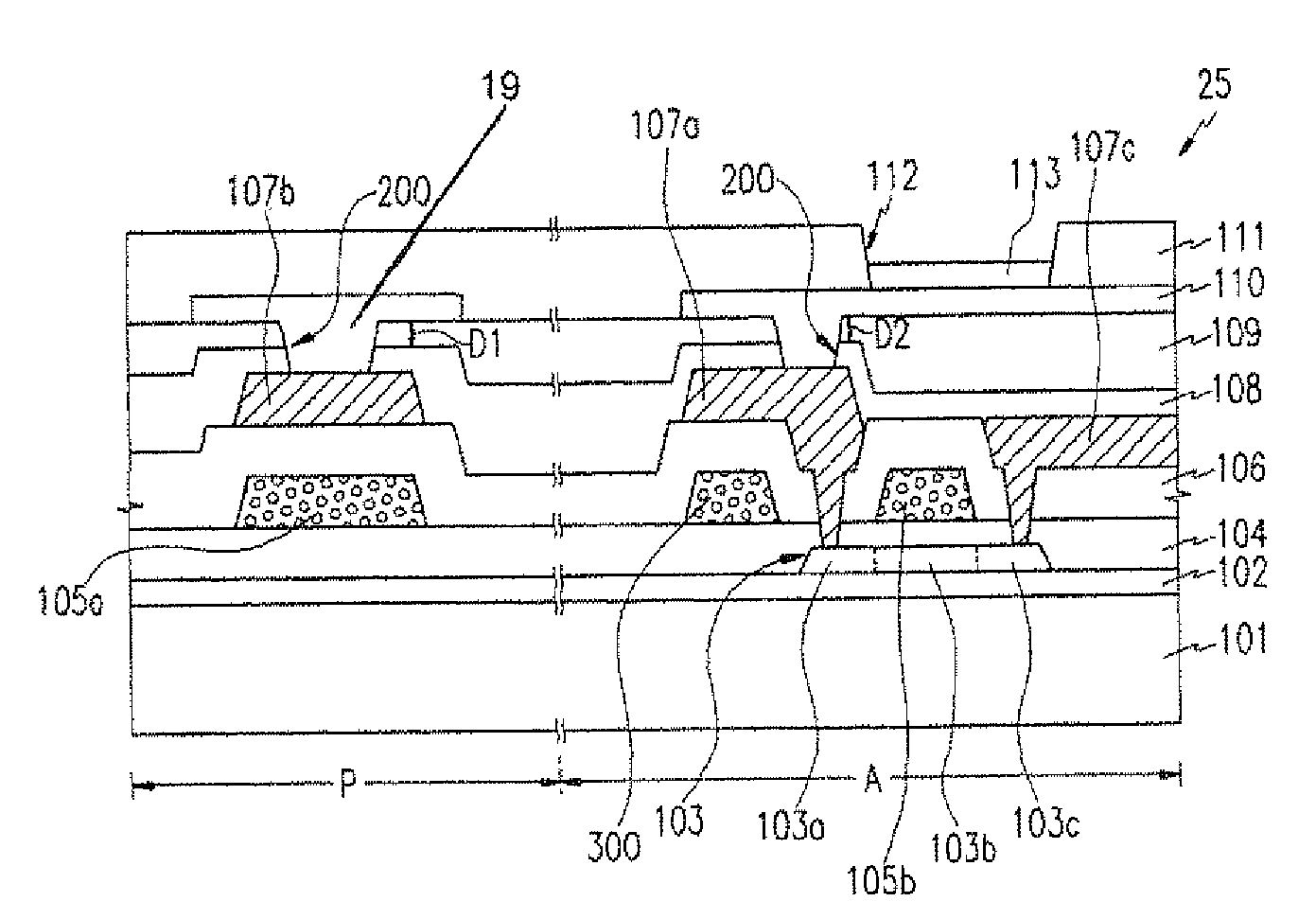
[0036]FIGS. 2 and 3 illustrate an organic EL display 25 configured in accordance with one exemplary embodiment of the present invention. The EL display 25 has a panel 17 with an array portion A for forming pixels, and a pad portion P located at the periphery thereof. Pads 19 are formed at the pad portion P to apply driving electrical signals to power transmission lines, scanning lines and data lines.

[0037]As shown in FIG. 3, the organic EL display 25 has a blocking layer 102 formed of SiO2 on an insulating substrate 101, and a polycrystalline silicon layer 103 having a predetermined width formed on the blocking layer 102.

[0038]N-type or p-type impurity ions are doped at the peripheries of the polycrystalline silicon layer 103 at a high concentration to form a lower drain region 103a and a lower source region 103c. The region between the lower drain region 103a and the lower source region 103c becomes a channel region 103b where electrons or holes migrate.

[0039]A gate insulating laye...


PUM


Abstract

An organic electroluminescent display includes a substrate having an array portion with pixels, and a pad portion coupled to an external power supply. A semiconductor structure is formed on the substrate with a source electrode, a drain electrode and a pad. A passivation layer is formed on the semiconductor structure with via holes exposing regions of the source and the drain electrodes at the array portion and the pad at the pad portion. Portions of the passivation layer contacting the via holes between the array portion and the pad portion have the same thickness. A conductive layer fills the via holes. A pixel defining layer is formed over the entire surface of a flattening layer and the conductive layer with pixel regions exposing regions of the conductive layer at the array portion. An organic electroluminescent film is formed at each pixel region.

Description

[0001]This application claims the benefit of Korean Patent Application No. 2003-0060016, filed on Aug. 28, 2003, which is hereby incorporated by reference for all purposes as if fully set forth herein.BACKGROUND OF THE INVENTION[0002]1. Field of the Invention[0003]The present invention relates to an organic electroluminescent display, and in particular, to an organic electroluminescent display that prevents pad electrodes from being over-etched by removing the thickness difference of a passivation layer including via holes between an array portion and a pad portion.[0004]2. Description of Related Art[0005]Generally, an electroluminescent (EL) display is a display device that utilizes the principle that electrons from a cathode and holes from an anode are injected into a light emission layer while being combined to form excitons, and the light emission layer emits light when the excitons go down from the excited state to the ground state.[0006]In contrast to a conventional thin film ...

Claims


Application Information

Patent Timeline
Patent Type & Authority Patents(United States)
IPC IPC(8): H01L29/04H01L29/15H01L31/036H01L51/50G09F9/30H01L21/77H01L21/84H01L27/32H05B33/22H05B44/00
CPCH01L27/3244H01L27/1248H01L27/3276H01L27/124H01L27/3248H01L27/3223H10K59/88H10K59/123H10K59/12H10K59/131H05B33/22
Inventor PARK, SANG-ILKANG, TAE-WOOK
Owner SAMSUNG DISPLAY CO LTD
Learn More