Insulated gate semiconductor device

a technology of semiconductor devices and gate semiconductors, which is applied in semiconductor devices, transistors, electrical devices, etc., can solve the problems of difficult to lower the on voltage, difficult to implement the above ideal concentration in the conventional manufacturing method of cstbt, etc., and achieve the effect of suppressing the variation of the threshold voltage (vgeth) and high concentration

Inactive Publication Date: 2007-05-01
MITSUBISHI ELECTRIC CORP
View PDF2 Cites 21 Cited by
  • Summary
  • Abstract
  • Description
  • Claims
  • Application Information

AI Technical Summary

Benefits of technology

[0034]According to the present invention, there can be provided the insulated gate semiconductor device having the above constitution, in which the gate capacity and the short-circuit current can be controlled, and the variation in the threshold voltage (VGEth) can be suppressed. Furthermore, although the CS layer region just under the channel is changed from N− layer to N+ layer because charges are stored when the gate voltage is applied, the CS layer region other than just under the channel can have a high concentration as much as possible in the CSTBT of the present invention, and therefore the ON voltage reduction can be implemented.

Problems solved by technology

However, it was difficult to implement the above ideal concentration in the conventional manufacturing method of the conventional CSTBT shown in FIGS. 19 to 23.
That is, it was difficult to lower the ON voltage.

Method used


Image

  • Insulated gate semiconductor device
  • Insulated gate semiconductor device
  • Insulated gate semiconductor device

Examples


embodiment 1

[0062](Embodiment 1)

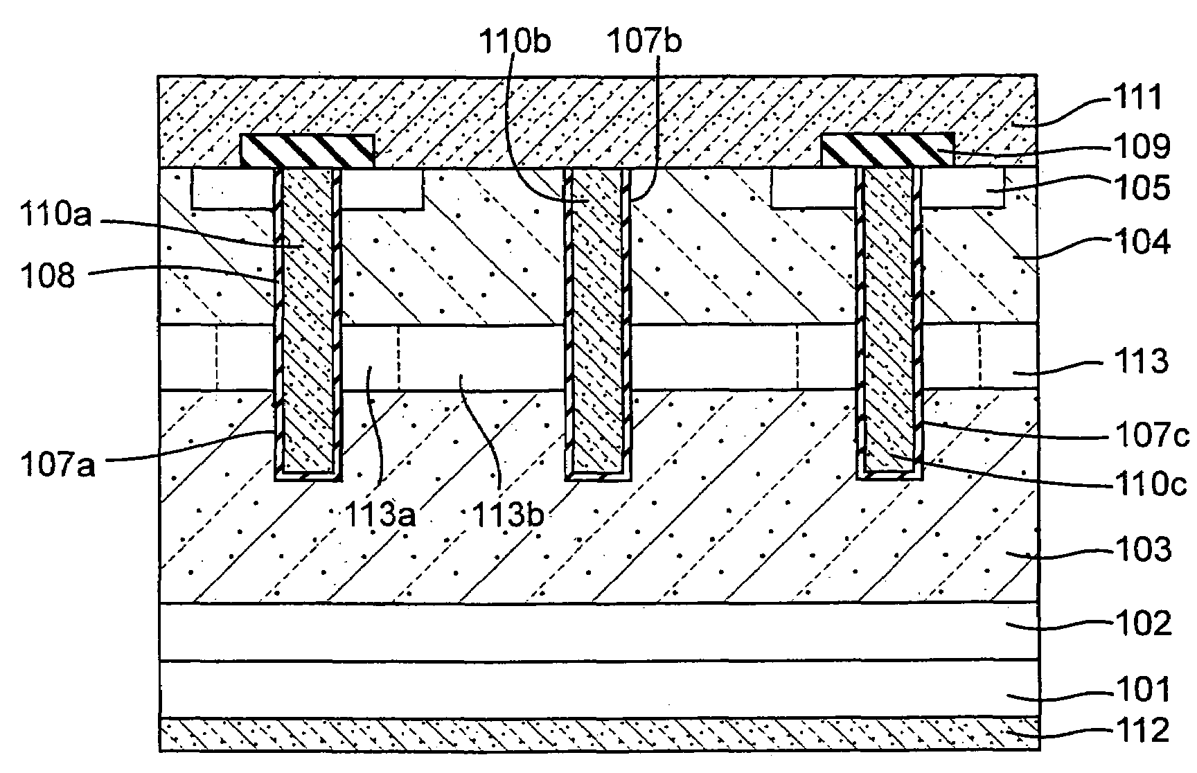
[0063]FIG. 1 is a sectional view schematically showing an example of a CSTBT according to an embodiment 1 of the present invention. In the CSTBT of the embodiment 1, a CS layer 113 comprises a first CS layer region 113a just under a channel region and a second CS layer region 113b other than just under the channel region, in which variation in threshold voltage (VGEth) is controlled by lowering an impurity concentration of the first CS layer region 113a. In addition, a carrier storing effect can be maintained by increasing a concentration of the second CS layer region 113b other than just under the channel region, so that an ON voltage can be lowered.

[0064]Its structure will be described with reference to FIG. 1 hereinafter. According to an illustrated constitution, an N+ buffer layer 102 is formed on a P+ substrate 101 which is a collector region, and a collector electrode 112 is formed on a back face of the P+ substrate 101. An N− semiconductor (base) layer 103...

embodiment 2

[0072](Embodiment 2)

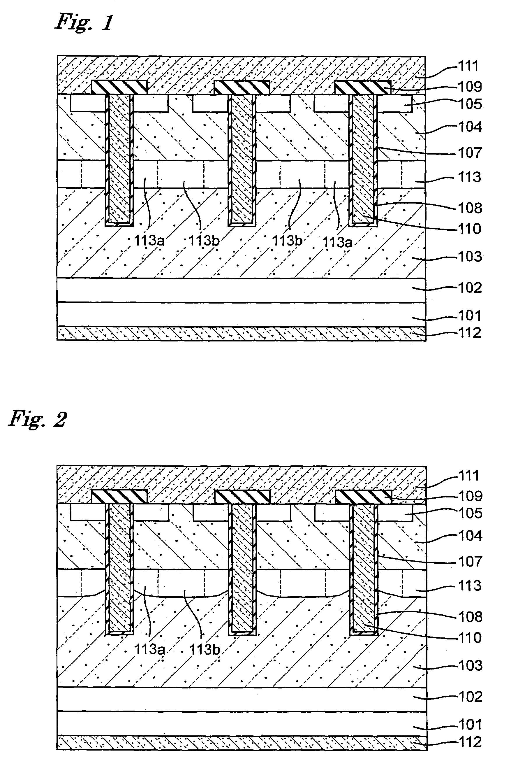
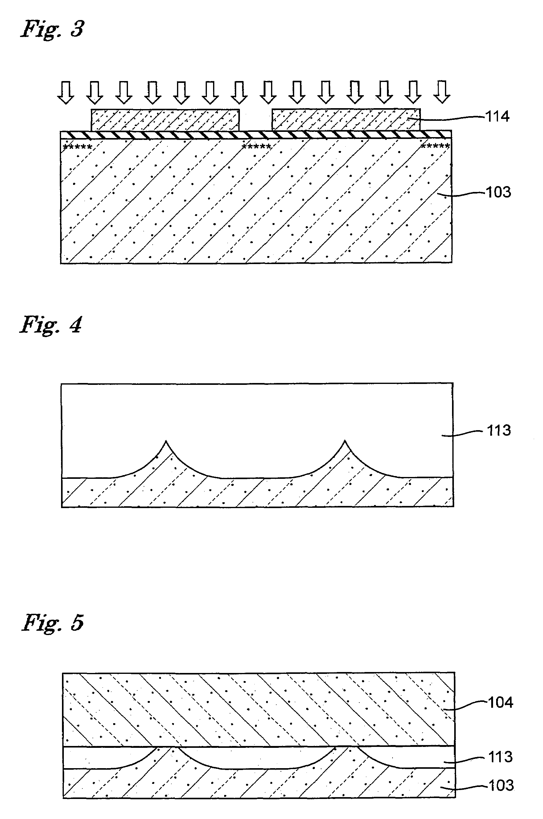
[0073]FIG. 2 is a sectional view schematically showing an example of a CSTBT according to an embodiment 2 of the present invention, and FIGS. 3 to 7 are schematic views showing a manufacturing flow from a step of forming a CS layer to a step of forming a trench gate in manufacturing of the CSTBT according to the embodiment 2. According to the CSTBT of the embodiment 2, a CS layer 113 comprises a first CS layer region 113a just under a channel region and in the vicinity of a sidewall of a trench, and a second CS layer region 113b other than just under the channel region. In this construction, the first CS layer region 113a is thinner than the second CS layer region 113b. By this arrangement, an impurity concentration of the first CS layer region 113a is lowered so that the variation in threshold voltage (VGEth) is controlled.

[0074]In addition, an impurity concentration of the second CS layer region 113b is made higher than that of the first CS layer region 113a, s...

embodiment 3

[0082](Embodiment 3)

[0083]FIG. 11 is a sectional view schematically showing an example of a CSTBT according to an embodiment 3 of the present invention. The CSTBT according to the embodiment 3 is a modified example of the embodiment 1 shown in FIG. 1, wherein a dummy trench gate is used as the second trench gate. That is, since a cell of a second trench gate electrode 110b is directly connected to an emitter electrode 111, a gate voltage VGE is 0V so that the second trench gate is a dummy gate region which does not function as a gate. Thus, there is an advantage that a withstand voltage is not lowered while a cell size is the same as that of the conventional TIGBT or CSTBT. Note that, in this embodiment, the phrase “second trench gate” means a dummy trench gate as defined in the above constitution.

[0084]For example, in the case where two trench gates out of three are connected to the emitter electrode 111 in a trench gate region formed in a stripe shape, a gate capacity and a short-...


PUM


Abstract

A CSTBT includes a carrier stored layer (113) formed between a P base region (104) and a semiconductor substrate (103) and the carrier stored layer has an impurity concentration higher than that of the semiconductor substrate (103). The P base region (104) in a periphery of a gate electrode (110) functions as a channel. When it is assumed that an impurity concentration of a first carrier stored layer region (113a) just under the channel is ND1 and an impurity concentration of a second carrier stored layer region (113b) other than just under the channel is ND2 in the carrier stored layer (113), the relationship of the impurity concentrations is defined by ND1<ND2. Thus, a gate capacity and a short-circuit current can be controlled and variation in threshold voltage can be prevented.

Description

BACKGROUND OF THE INVENTION[0001]1. Field of the Invention[0002]The present invention relates to an insulated gate semiconductor device, and more particularly, relates to an insulated gate semiconductor device such as a bipolar transistor and a power MOSFET having an insulated gate, in which an excessive short-circuit current is controlled by suppressing a voltage rise between a gate and an emitter, which occurs when a switching operation is performed at a time of short-circuiting such as a load.[0003]2. Description of the Related Art[0004]In a general power electronics device for driving a motor and the like, a power semiconductor element of such as an insulated gate bipolar transistor (referred to as “IGBT” hereinafter) is mainly used as a switching element in a region where a rated voltage is 300V or more because of its characteristics. Especially, a lot of attention has been lately attracted to an insulated gate semiconductor device having a trench gate, that is, an insulated ga...

Claims


Application Information

Patent Timeline
Patent Type & Authority Patents(United States)
IPC IPC(8): H01L29/74H01L31/111H01L29/78H01L21/331H01L27/082H01L27/102H01L29/08H01L29/10H01L29/70H01L29/739H01L29/76H01L29/94H01L31/062H01L31/11H01L31/113H01L31/119
CPCH01L29/0834H01L29/7397H01L29/66348H01L29/1095H01L29/1004
Inventor TOMOMATSU, YOSHIFUMITAKAHASHI, HIDEKITADOKORO, CHIHIRO
Owner MITSUBISHI ELECTRIC CORP
Why Eureka
Try Eureka