Mask ROM

a technology of mask and rom, applied in the field of mask rom, can solve the problems of large parasitic capacitance generated in the virtual gnd line, increased power consumption, and longer driving time, and achieve the effects of reducing power consumption, improving data reading accuracy, and reducing leakage current from non-selected cell transistors

Inactive Publication Date: 2007-05-15
SOCIONEXT INC
View PDF18 Cites 12 Cited by
  • Summary
  • Abstract
  • Description
  • Claims
  • Application Information

AI Technical Summary

Benefits of technology

[0007]The virtual GND line has to serve as a ground line when the virtual GND line is read, and serve as a control line for separating non-selected bit cells from a selected bit cell when the virtual GND line is not selected. Therefore, for example, to read a single memory cell, each of the potential of a single selected bit line and the potential of a single non-selected source line has to be changed from the ground line level to the power supply voltage level. Thus, as a large parasitic capacitance is generated in a virtual GND line (i.e., source line), power consumption is increased. Moreover, compared to the case where a parasitic capacitance is small, a longer driving time is required. This results in increase in access time in the mask ROM.
[0023]Furthermore, in a source node section according to the present invention, a source portion is shared only between first and second transfer gate transistors connected to the same first word line or between third and fourth transfer gate transistors connected to the second word line located adjacent to the first word line. With the source portion so configured to be independent from another source portion for each one of plurality of bit lines connected to the first, second, third and fourth transfer gate transistors, respectively, a floating capacitance of the source node section of which a potential is needed to be changed can be reduced, thus resulting in reduction in power consumption and driving time.

Problems solved by technology

However, a virtual GND scheme realized in the known mask ROM has the following problems.
A first problem is that a large parasitic capacitance is generated in a virtual GND line.
Thus, as a large parasitic capacitance is generated in a virtual GND line (i.e., source line), power consumption is increased.
Moreover, compared to the case where a parasitic capacitance is small, a longer driving time is required.
This results in increase in access time in the mask ROM.
A second problem is that because of the necessity to provide interconnects such that two interconnects, i.e., a bit line and a source line as a pair extend in the same direction, each of the bit line and the source line is shared by adjacent two bit cells in the direction in which word lines extend.
Accordingly, in the known mask ROM, a single contact is shared by adjacent bit cells and, therefore, it is difficult to write information into a single transistor for each a bit line contact or a source line contact.

Method used


Image

  • Mask ROM
  • Mask ROM
  • Mask ROM

Examples


examples

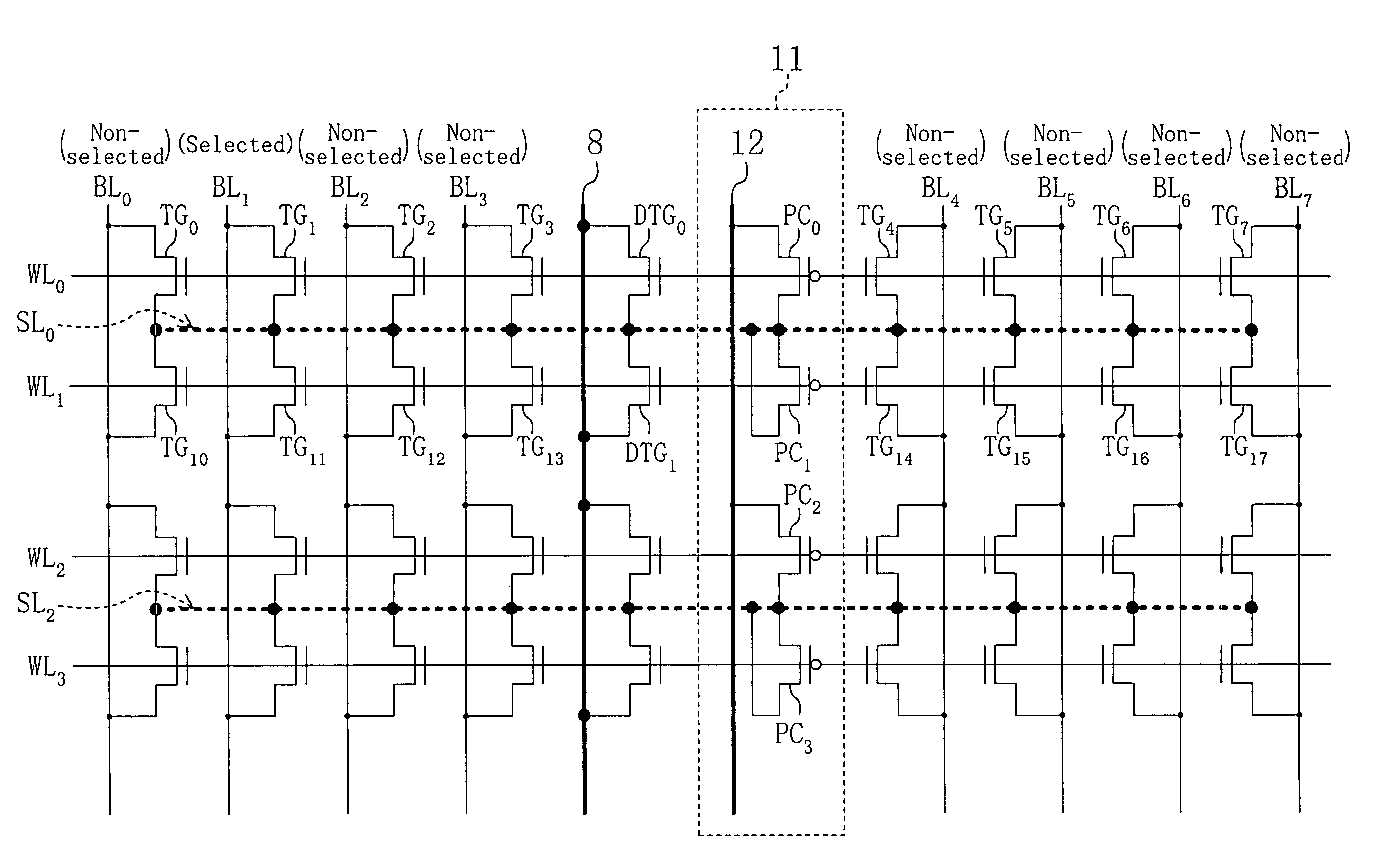
[0063]FIG. 12 is a circuit diagram of a mask ROM according to a first modified example of this embodiment.

[0064]In the mask ROM of the first modified embodiment has the similar configuration as that of the mask ROM of FIG. 2 except for the point that a source pre-charging circuit 11 for pre-charging a source of a non-selected cell transistor to a power supply potential in advance is provided. Hereinafter, feature part of the first modified example will be described.

[0065]The source pre-charging circuit 11 includes, for example, p-channel transistors PC0, PC1, PC2, . . . . Gates of the p-channel transistors PC0, PC1, PC2, . . . are connected to word lines WL0, WL1, WL2 . . . , respectively. Drains of any two of the transistors located adjacent each other (for example, a transistor PC0, i.e., a second field effect transistor, and a transistor PC1, i.e., a third field effect transistor) are connected to each other. Moreover, a source of one of the adjacent two transistors (for example,...


PUM


Abstract

A mask ROM includes bit lines, word lines intersecting with the bit lines and bit cells provided along the word lines, each of the bit lines being formed of a cell transistor having a gate connected to an associated one of the word lines. In the mask ROM, further provided is a source node commonly connected to respective sources of ones of the cell transistors having a gate connected to one of adjacent two word lines. A current flows from a selected bit line to a non-selected bit line via a cell transistor selected in reading out data and the source node.

Description

CROSS-REFERENCE TO RELATED APPLICATION[0001]This application claims priority under 35 U.S.C. §119(a) on Japanese Patent Application No. 2004-142515 filed on May 12, 2004, the entire contents of which are hereby incorporated by reference.BACKGROUND OF THE INVENTIONField of the Invention[0002]The present invention relates to a mask ROM programmed by connection / disconnection between a bit line and a drain.[0003]As a read-only memory which requires a short time (i.e., turn around time which will be referred to as a “TAT”) from a time when information to be written is received from a user to a time when a product is supplied, a mask ROM has been widely used.[0004]In a general mask ROM, bit lines BL0, BL1, . . . , word lines intersecting the bit lines and a plurality of bit cells each of which is formed of a single cell transistor are provided. Information is read according to whether or not bit line connection is present or not in each of the bit cells (see a left drawing in FIG. 1). Mor...

Claims


Application Information

Patent Timeline
Patent Type & Authority Patents(United States)
IPC IPC(8): G11C17/00G11C5/06G11C17/12H01L21/8246H01L27/112
CPCG11C17/12H01L27/112H10B20/00
Inventor YAMAUCHI, HIROYUKI
Owner SOCIONEXT INC
Why Eureka
Try Eureka