Memory device having redundant memory for repairing defects

a memory device and defect technology, applied in the field of memory devices, can solve the problems of reducing production yield, memory chips must be scrapped as poor products, and normal storage operation cannot be enabled, and achieve the effect of reducing size and speed

Active Publication Date: 2007-05-15
SHARP KK
View PDF9 Cites 21 Cited by
  • Summary
  • Abstract
  • Description
  • Claims
  • Application Information

AI Technical Summary

Benefits of technology

[0020]An object of the invention is to provide a memory device that defective points of another memory chip can be repaired by means of a control logic simple and high in speed and wherein the memory chip thereof can be reduced in size.
[0024]In this manner, the defective point in the storage means is repaired by the redundant storage means of another of mounting means. Furthermore, by stacking the memory mounting members, time difference in signal propagation is extremely reduced, thereby eliminating the necessity of a control logic that takes account of a time difference. Accordingly, it is possible to realize a control logic simple and high in speed and to repair a defective point in the memory chip that is another of memory mounting members.
[0025]According to the invention, because the defect point in the storage means is repaired by the redundant storage means of the first or second memory chip other than the memory chip as the memory mounting member of the storage means having the defect, memory chip yield can be improved. Furthermore, because time difference in signal propagation is made extremely small by stacking the first memory chips and the second memory chip three-dimensionally in a direction of thickness thereof, there is eliminated the need for a control logic that takes account of a time difference, thus making it possible to realize a control logic simple and high in speed.
[0029]According to the invention, the first memory mounting member has solely storage means to thereby eliminate the redundant means. The redundant storage means and control means are mounted only on one second memory mounting member. Accordingly, the memory chip can be further reduced in size.
[0030]Further, according to the invention, the memory device is composed of first memory chips having solely storage means for storing data, and a second memory chip having control means for memory control and redundant storage means for repairing a defect in the storage means of the first memory chip. Accordingly, there is no need to mount the control means and the redundant storage means on each of the memory chips, thus making it possible to further reduce the size of the memory chips.

Problems solved by technology

In the memory chip, erroneous bits possibly occur as defects that disable normal storage operation because of a trouble encountered in the process.
In the case there is an erroneous bit even one in the number on a memory chip, the memory chip must be scrapped away as a poor product.
This results in a lowering in production yield.
Consequently, there arises memory chips not to be repaired with redundancy, i.e. memory chips unavoidably scrapped away as unacceptable products, at a certain probability.
The memory to be read destructively, as represented by the DRAM (dynamic random access memory), requires complicated control, e.g. repairing the data destroyed upon reading by post-read rewrite.
Even in an electrically erasable memory such as a flash memory, complicated control is needed including to supply, as a write operation voltage, a voltage different from the reading operation voltage, and allow operation while monitoring a write completion, and so on.
Because such a memory cell as a pseudo SRAM or a flash memory requires complicated control as noted above, many electric interconnections are needed between the logic for memory control and the memory cells.
For this reason, the terminals increased in the number are not easily accommodated in the conventional semiconductor package.
Thus, it is not easy to adopt mounting the logic for memory control and those memory cells on different memory chips.
It takes a time in signal propagation correspondingly to the planar size of the memory chip, causing a time difference in the time to receive signals at the individual memory chips.
Thus, there is a problem that the chips cannot be reduced down to a size required to secure a constant value or higher of yield.
There is a problem that, even where there are available redundant memories of other memory chips, the memory chip is to become poor unless repaired by the redundant memory of the relevant memory chip.
However, there is a problem that the memory chip increases in size because the memory, the memory controlling logic and the redundant memory are mounted on the memory chip.

Method used


Image

  • Memory device having redundant memory for repairing defects
  • Memory device having redundant memory for repairing defects
  • Memory device having redundant memory for repairing defects

Examples


first embodiment

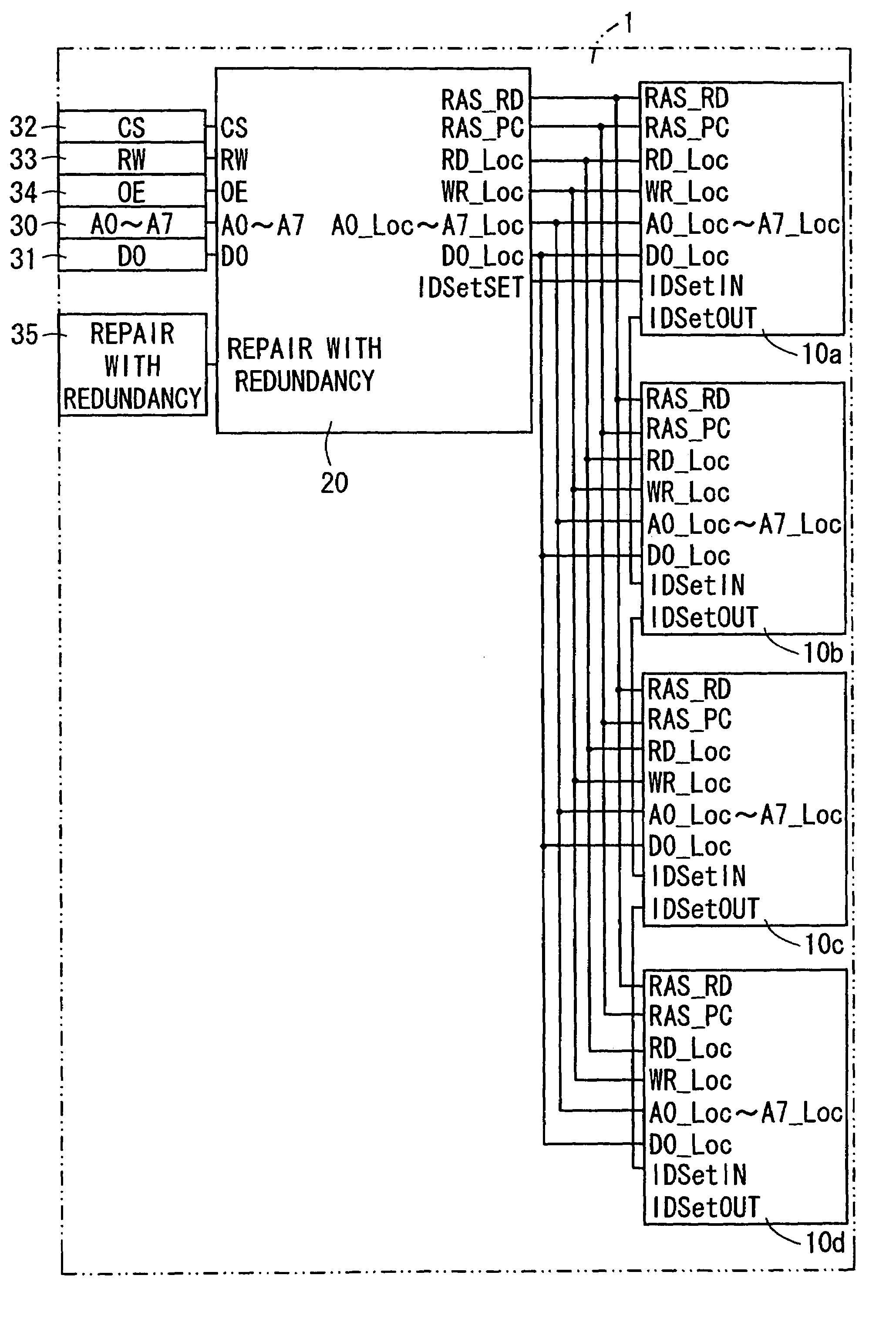
[0067]FIG. 1 is a diagram showing a circuit configuration of a memory device 1 in the invention. Storage is explained as a DRAM in scheme. The memory device 1 includes first memory chips 10a, 10b, 10c and 10d (hereinafter, sometimes collectively referred as a first memory chip 10), as a first memory mounting member, and a second memory chip 20, as a second memory mounting member.

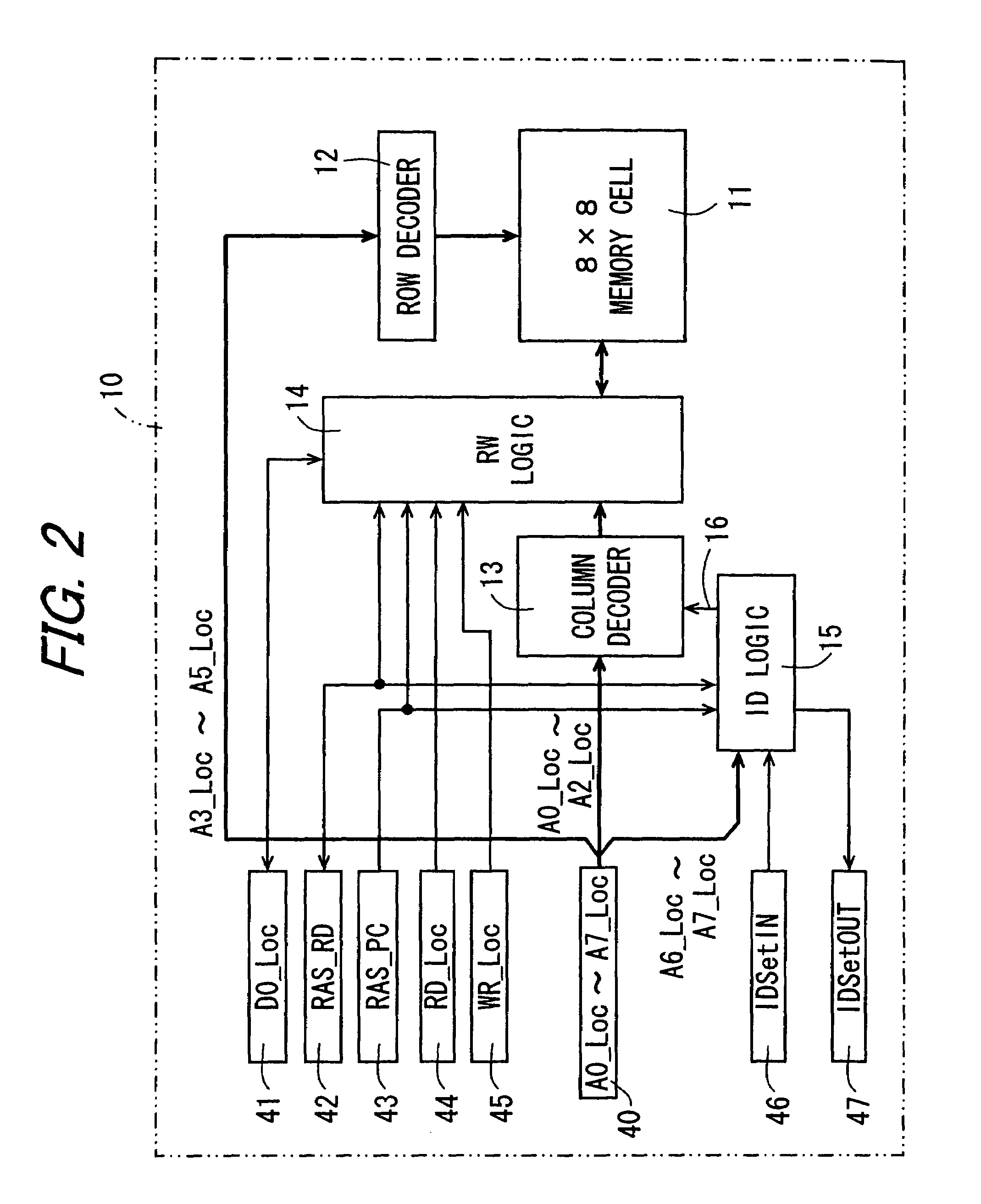
[0068]The first memory chips 10a to 10d each have a memory cell as storage means for storing data, without having a redundant memory cell as redundant storage means for repairing an erroneous bit as a defect in the memory cell. Furthermore, a logic minimal in degree is solely provided to operate on a control logic as control means in the second memory chip.

[0069]The second memory chip 20 has a control logic as a logic for effecting memory control of the memory cells and the redundant memory cells, and a redundant memory cell for repairing an error bit of the first memory chips 10a to 10d. This control logic ...

second embodiment

[0087]FIG. 6 is a diagram showing a circuit configuration of a memory device 2 in the invention. The memory device 2 includes first memory chips 100a, 100b, 100c and 100d (hereinafter sometimes collectively referred as a first memory chip 100), as first memory carrier means, and a second memory chip 200, as second memory mounting member. The difference from the memory device 1 shown in FIG. 1 lies in an increase of signals CS0_Loc to CS3_Loc and IDSetCK at between the first memory chips 100a to 100d and the second memory chip 200.

[0088]FIG. 7 is a diagram showing a circuit configuration example of the first memory chip 100 shown in FIG. 6. The first memory chip 100 has a chip select terminal 49 which is chip select means allowing to select one out of the first memory chips. The same functional elements as those of the first memory chip shown in FIG. 2 are attached with the same references, to omit duplicated explanations.

[0089]An A0_Loc–A5_Loc terminal 400 is an address terminal. De...


PUM


Abstract

First memory chips each have a memory cell as storage means for storing data and do not have a redundant memory cell as redundant storage means for repairing an erroneous bit in the memory cell. Furthermore, a logic minimal in degree is solely provided for operation on a control logic of a second memory chip. The second memory chip has a control logic for effecting memory control of the memory cells, the redundant memory cells, etc. and a redundant memory cell for repairing an error bit of the first memory chips. The memory device is structured by stacking the first and second memory chips.

Description

CROSS-REFERENCE TO RELATED APPLICATION[0001]This application claims priority to Japanese Patent Application No. JP 2004-267341, which was filed on Sep. 14, 2004, and the contents of which are incorporated herein by reference, in their entirety.BACKGROUND OF THE INVENTION[0002]1. Field of the Invention[0003]The present invention relates to a memory device that defects of a memory possessed by a memory chip can be repaired.[0004]2. Description of the Related Art[0005]In the memory chip, erroneous bits possibly occur as defects that disable normal storage operation because of a trouble encountered in the process. In the case there is an erroneous bit even one in the number on a memory chip, the memory chip must be scrapped away as a poor product. This results in a lowering in production yield.[0006]FIG. 21 is a block diagram showing a configuration of a memory chip 80 applied with the related art. The memory chip 80 includes a memory cell 81, a row decoder 82, a column decoder 83, a re...

Claims


Application Information

Patent Timeline
Patent Type & Authority Patents(United States)
IPC IPC(8): G11C29/00
CPCG11C5/02G11C5/04G11C29/808G11C29/785
Inventor SATOH, TOMOTOSHI
Owner SHARP KK
Why Eureka
Try Eureka