Method of forming patterns

a pattern and pattern technology, applied in the field of pattern formation, can solve the problem of inability to obtain accurate resist patterns, and achieve the effect of high degree of accuracy and sufficient mechanical strength

Inactive Publication Date: 2007-05-29
ADTEC ENG +1
View PDF3 Cites 5 Cited by
  • Summary
  • Abstract
  • Description
  • Claims
  • Application Information

AI Technical Summary

Benefits of technology

[0007]The present invention has been developed in view of the circumstances described above. Accordingly, it is the primary object of the present invention to provide a pattern forming method that is capable of preventing a reduction in the yield rate due to damaged resist patterns, and also capable of accurately forming desired patterns.
[0012]The pattern-forming method of the present invention employs an N-layer mask pattern as a mask for etching. Since the N-layer mask pattern has sufficient mechanical strength compared with a mask pattern of a single-layer structure, there is no possibility that the N-layer mask pattern will tear in the development and etching steps. In addition, the N-layer mask pattern becomes smaller in pattern size from the bottom layer toward the top layer so that a wide gap is formed between the underlying layer and the overlying layer, so there is no possibility that the flow of an etchant will be blocked in an etching step. Thus, in the etching step, a pattern of the same shape as the first pattern (bottom layer) of the N-layer-mask pattern can be formed on a substrate with a high degree of accuracy.

Problems solved by technology

For this reason, there are cases where accurate resist patterns cannot be obtained.

Method used


Image

  • Method of forming patterns
  • Method of forming patterns
  • Method of forming patterns

Examples


Embodiment Construction

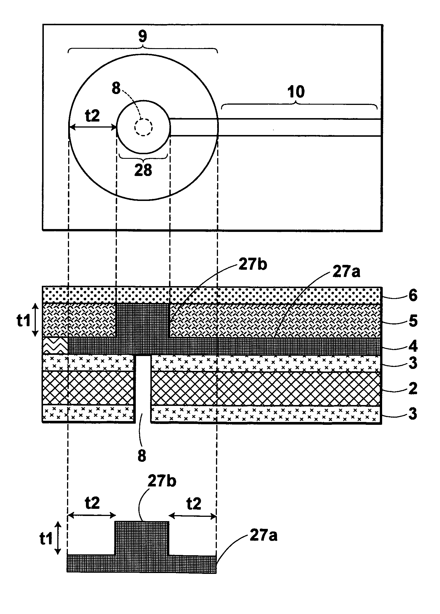
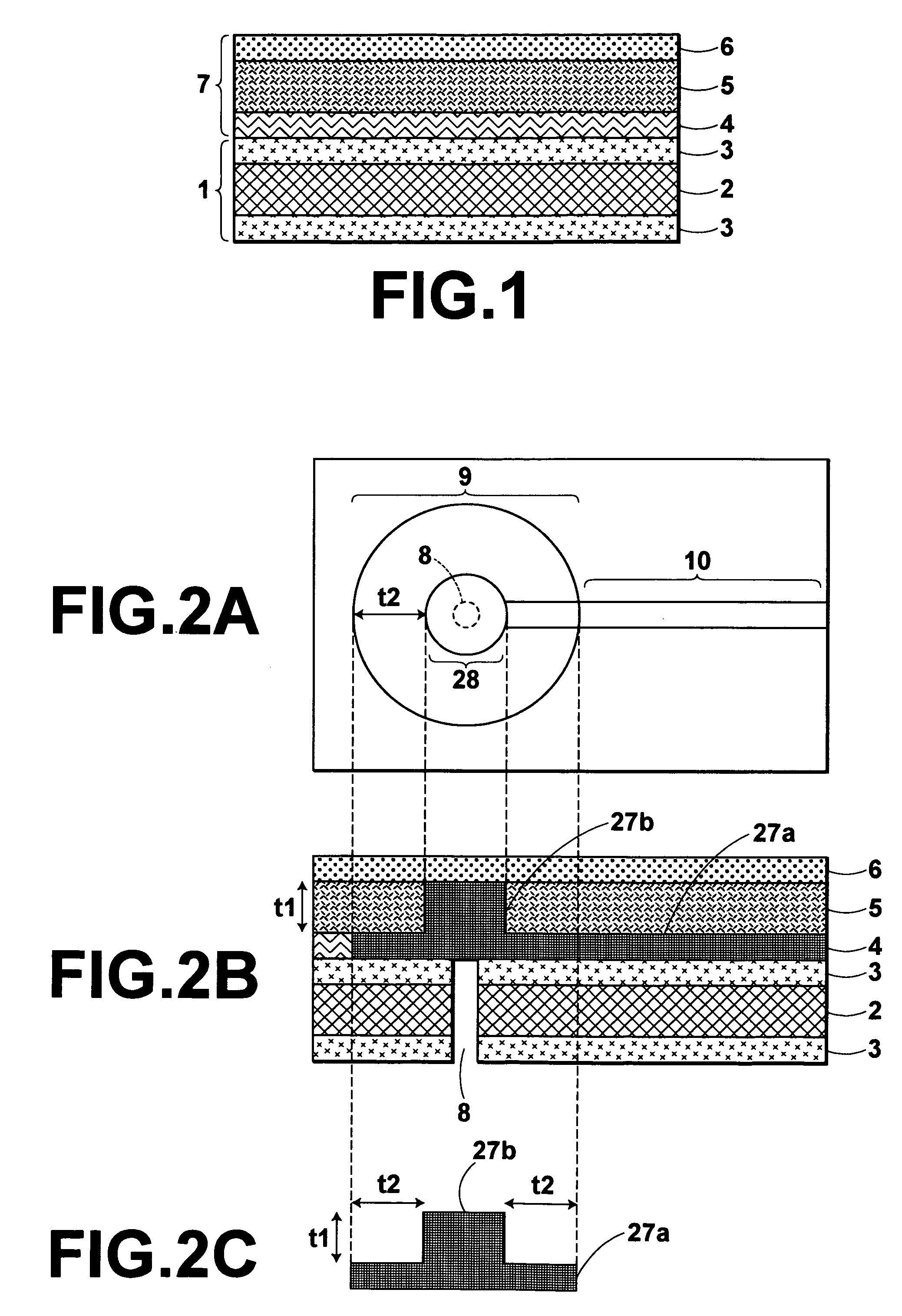
[0042]As a preferred embodiment of an image recording method of the present invention, a description will hereinafter be given of a pattern recording method used when recording wiring patterns on a substrate in a printed-circuit board fabrication step.

[0043]FIG. 1 shows a substrate 1 on which wiring patterns are to be formed. A resist film 7 has been stuck on the substrate 1.

[0044]As shown in FIG. 1, the substrate 1 comprises a glass epoxy substrate material 2, and thin copper films 3 stacked on both surfaces of the substrate material 2. The resist film 7 comprises a support layer 6, a thick-film low-photosensitive layer 5 (hereinafter referred to as a thick photosensitive layer 5) stacked on the support layer 6, and a thin-film highly-photosensitive layer 4 (hereinafter referred to as a thin photosensitive layer 4) stacked on the thick photosensitive layer 5. As shown in FIG. 1, the resist film 7 is stuck on the substrate 1 so that the thin photosensitive film 4 is contacted with t...


PUM

PropertyMeasurementUnit
thicknessaaaaaaaaaa
thicknessaaaaaaaaaa
thicknessaaaaaaaaaa

Abstract

In forming a mask pattern on a circuit board, a mask pattern of N-layer structure is formed in a region where the mechanical strength of the circuit board needs to be increased. N photosensitive layers are first stacked on a substrate so that they becomes lower in sensitivity from the first photosensitive layer toward the Nth photosensitive layer. In the first photosensitive layer (bottom layer), a first pattern is formed and has the same shape as a predetermined pattern to be formed on the circuit board. In the Kth photosensitive layer (N≧K≧2), a Kth pattern is formed so that the Kth pattern is smaller than a (K−1)st pattern formed in the (K−1)st photosensitive layer and arranged inside the (K−1)st pattern.

Description

BACKGROUND OF THE INVENTION[0001]1. Field of the Invention[0002]The present invention relates to a method suitable for forming wiring patterns on a substrate during a printed-circuit board fabrication step.[0003]2. Description of the Related Art[0004]Wiring patterns for a printed circuit board are typically formed as follows. First, a resist layer comprising a photosensitive material is formed on a conductive layer (e.g., a thin film of Cu) on which wiring patterns are to be formed. Then, the resist layer is exposed with a mask having patterns of the same shapes as the wiring patterns. After patterns of the same shapes as the wiring patterns (hereinafter referred to as resist patterns) are formed in the resist layer by development, the conductive layer is etched with the resist patterns as a mask. In this manner, the wiring patterns are formed on the conductive layer.[0005]When fabricating a double-sided (or multilayer) printed circuit board, a through hole is first formed to connec...

Claims


Application Information

Patent Timeline
Patent Type & Authority Patents(United States)
IPC IPC(8): H01L21/302G03F7/26G03F7/095H05K3/00H05K3/06
CPCG03F7/095H05K3/0079H05K3/064H05K3/0082H05K2203/0577H05K2203/0588Y10S438/975Y10S438/95
Inventor SASAKI, YOSHIHARU
Owner ADTEC ENG
Why Eureka
Try Eureka