Gamma ray detector modules

a detector module and gamma ray technology, applied in the direction of x/gamma/cosmic radiation measurement, radioation controlled devices, instruments, etc., can solve the problems of low-temperature soldering alone, inapplicability to many applications, and high cost, so as to reduce assembly operations, reduce the number of assembly operations, and reduce the effect of assembly operations

Inactive Publication Date: 2007-05-29
CREATIVE ELECTRON
View PDF55 Cites 72 Cited by
  • Summary
  • Abstract
  • Description
  • Claims
  • Application Information

AI Technical Summary

Benefits of technology

[0016]2. By employing the inventive interposer and low-temperature encapsulated solder joint approach, it is possible to eliminate the lower plate of the prior art. This reduces the number of assembly operations as well as provides a low profile module.
[0017]An interposer is a high-density printed circuit that interconnects a detector array to one or more readout chips or devices. It also interconnects the detector to a connector for interconnecting the detector module's I/O, power and ground circuits to signal processing electronics and power sources on a motherboard or backplane. The interposer eliminates

Problems solved by technology

The soldering of such bumps can also be accomplished at temperatures below 120 degrees C. The limitation of using such low-temperature solder is that the solder joints formed are relatively weak and subject to cracking and breaking.
Therefore, the use of low-temperature solders alone, as proposed in the prior art, is not practical for many applications.
Another issue is that creation of large detectors requires a package that allows detectors modules to be abutted together into large tiled arrays, without dead space in between detector modules.
One problem with prior art approaches that use of indium bump bonding to bond the various elements electrically is that the indium bump bond

Method used


Image

  • Gamma ray detector modules
  • Gamma ray detector modules
  • Gamma ray detector modules

Examples


Embodiment Construction

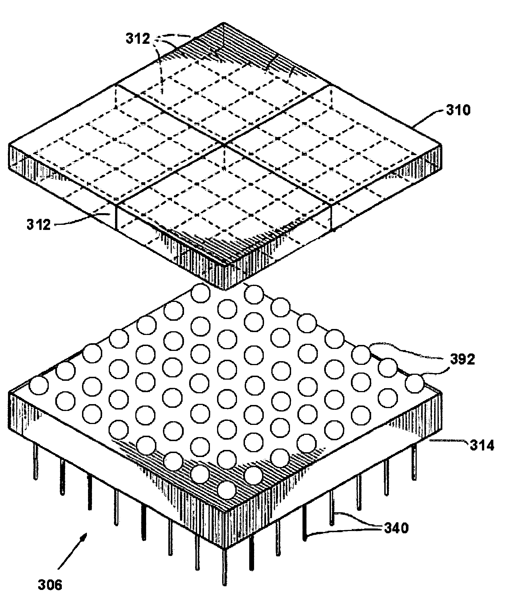
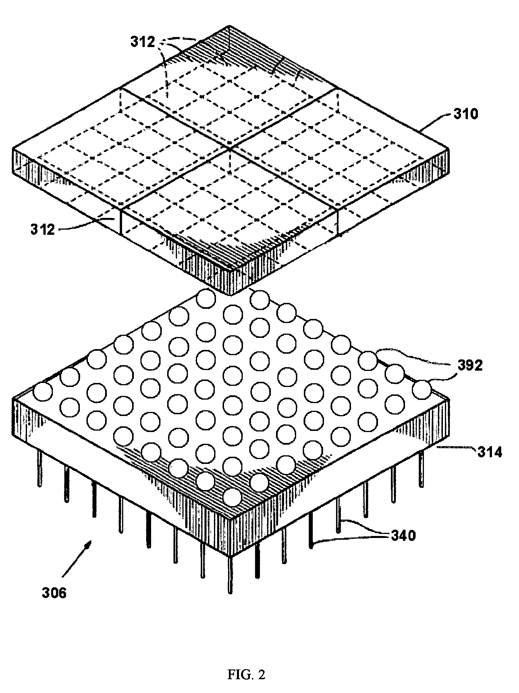
[0022]FIG. 2 shows a perspective view of a detection module 306 of the present invention. As depicted in FIG. 2, the detection module 306 comprises an integrated circuit mounted within a ceramic or plastic interposer circuit card 314. The semiconductor detector 310 of the detection module 306 includes an array of detection elements 312. A plurality of solder bumps 392 provide electrical connection for each detection element 312 to a corresponding input contact pad on the top surface of the interposer 314. The solder bumps 392 are electrically isolated from each other by a solid encapsulating material (not shown).

[0023]In the preferred embodiment of the present invention, the detection elements 312 comprise a plurality of cadmium-zinc-telluride (CZT) gamma-ray detection areas formed on the lower surface of detector 310. The detectors can alternatively comprise cadmium telluride, or other x-ray or gamma-ray sensitive materials. The detectors convert x-rays and gamma rays into electric...


PUM


Abstract

A radiation detector assembly has a semiconductor detector array substrate of CdZnTe or CdTe, having a plurality of detector cell pads on a first surface thereof, the pads having a contact metallization and a solder barrier metallization. An interposer card has planar dimensions no larger than planar dimensions of the semiconductor detector array substrate, a plurality of interconnect pads on a first surface thereof, at least one readout semiconductor chip and at least one connector on a second surface thereof, each having planar dimensions no larger than the planar dimensions of the interposer card. Solder columns extend from contacts on the interposer first surface to the plurality of pads on the semiconductor detector array substrate first surface, the solder columns having at least one solder having a melting point or liquidus less than 120 degrees C. An encapsulant is disposed between the interposer circuit card first surface and the semiconductor detector array substrate first surface, encapsulating the solder columns, the encapsulant curing at a temperature no greater than 120 degrees C.

Description

RELATED APPLICATIONS[0001]This patent application claims the benefit of Provisional U.S. Patent Application Ser. No. 60 / 430,659 filed Dec. 4, 2002.[0002]The captioned invention was developed under the United States of America Department of Health and Human Services Grant 1R43CA96023.FIELD OF THE INVENTION[0003]The invention relates to x-ray or gamma ray detection devices and gamma ray imaging devices comprising a semiconductor detector substrate including a plurality of detector elements interconnected to an interposer card. The interposer card is in turn interconnected to a readout device (e.g. a semiconductor readout device) that is mounted on the interposer card, the readout device including a corresponding plurality of readout cells. The interposer card further includes one or more connectors for interconnecting the device to power, ground and other signal processing electronics.BACKGROUND OF THE INVENTION[0004]A semiconductor detector substrate used for detection of x-rays and ...

Claims


Application Information

Patent Timeline
IPC IPC(8): H01L25/00
CPCH01L27/14634H01L27/14636H01L27/1469H01L31/0296H01L27/14658
Inventor CAPOTE, M. ALBERTLENOS, HOWARD A.
Owner CREATIVE ELECTRON
Why Eureka
Try Eureka