Method of forming a floating metal structure in an integrated circuit

a metal structure and integrated circuit technology, applied in the direction of resistors, basic electric elements, solid-state devices, etc., can solve the problems of limited signal propagation speed in integrated circuits, inconvenient control of air gaps between metal lines, and inability to form air gaps resulting from air gaps

Inactive Publication Date: 2007-06-05
MONTEREY RES LLC
View PDF41 Cites 4 Cited by
  • Summary
  • Abstract
  • Description
  • Claims
  • Application Information

AI Technical Summary

Benefits of technology

[0009]The present invention relates to a novel method of forming a floating metal structure in an integrated circuit. In one embodiment, a dielectric region separates a floating metal structure from an underlying substrate or another floating metal structure. The dielectric region is an air core rat

Problems solved by technology

The speed at which a signal is propagated in an integrated circuit is limited by the delay through the interconnect line carrying the signal.
The inability of the TEOS oxide to completely fill the

Method used


Image

  • Method of forming a floating metal structure in an integrated circuit
  • Method of forming a floating metal structure in an integrated circuit
  • Method of forming a floating metal structure in an integrated circuit

Examples


Embodiment Construction

[0020]In the present disclosure, numerous specific details are provided, such as examples of apparatus, process parameters, thicknesses, materials, steps, and structures to provide a thorough understanding of embodiments of the invention. Persons of ordinary skill in the art will recognize, however, that the invention can be practiced without one or more of the specific details, or with other apparatus, process parameters, thicknesses, materials, steps, and structures. In other instances, well-known details are not shown or described to avoid obscuring aspects of the invention.

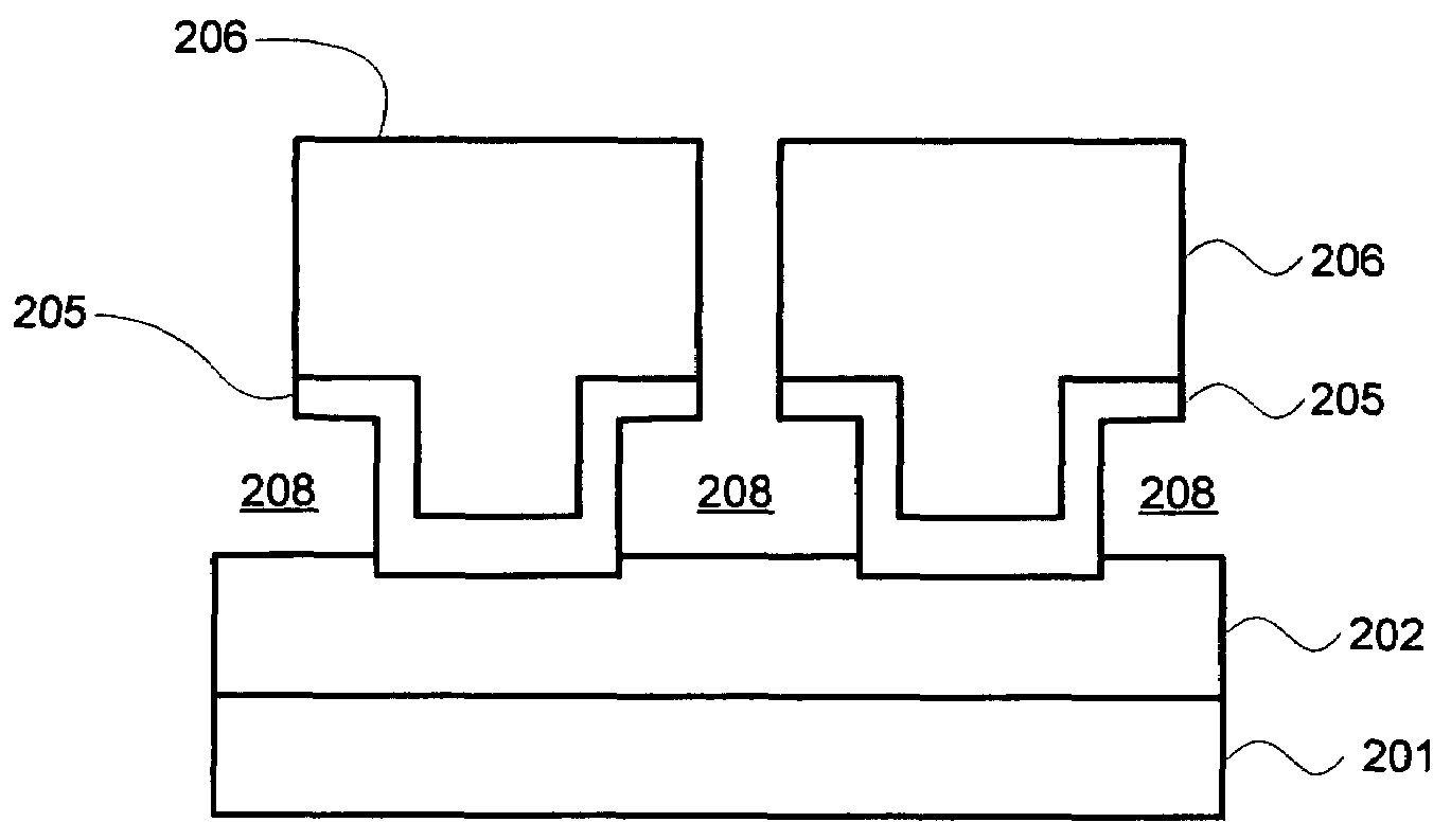
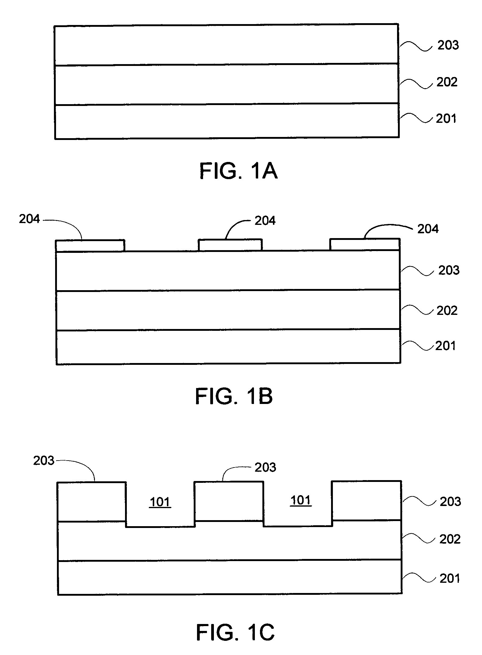
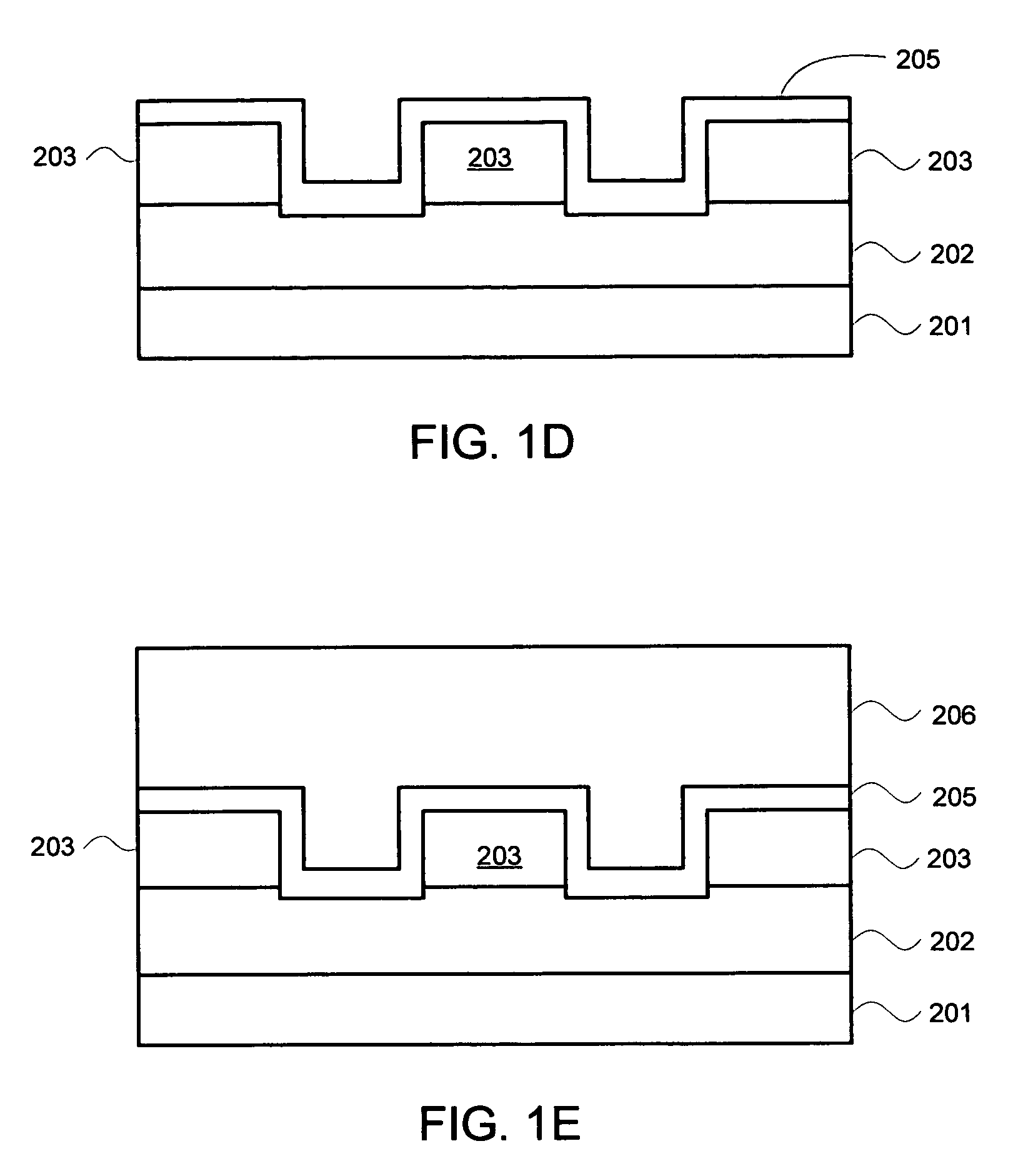
[0021]A method of forming a floating metal structure in an integrated circuit in accordance with an embodiment of the present invention is now described with reference to the sectional views of FIGS. 1A–1H. In FIG. 1A, a base layer 202 is deposited on a substrate 201. Base layer 202 provides a support on which a floating metal structure is formed. In some applications, a base layer may not be required; in that...


PUM


Abstract

In one embodiment, a sacrificial layer is deposited over a base layer. The sacrificial layer is used to define a subsequently formed floating metal structure. The floating metal structure may be anchored into the base layer. Once the floating metal structure is formed, the sacrificial layer surrounding the floating metal structure is etched to create a unity-k dielectric region separating the floating metal structure from the base layer. The unity-k dielectric region also separates the floating metal structure from another floating metal structure. In one embodiment, a noble gas fluoride such as xenon difluoride is used to etch a sacrificial layer of polycrystalline silicon.

Description

REFERENCE TO RELATED APPLICATION[0001]This application is a divisional of U.S. application Ser. No. 10 / 059,823, filed on Jan. 29, 2002, which is incorporated herein by reference in its entirety now U.S. Pat. No. 6,835,616.BACKGROUND OF THE INVENTION[0002]1. Field of the Invention[0003]The present invention relates generally to integrated circuit fabrication, and more particularly to processes for forming metal structures in integrated circuits.[0004]2. Description of the Background Art[0005]The speed at which a signal is propagated in an integrated circuit is limited by the delay through the interconnect line carrying the signal. This delay, commonly known as “RC delay,” is due to the resistance and capacitance of the interconnect line. Reducing the resistance or capacitance of an interconnect line lowers its RC delay and increases signal propagation speed. Thus, reducing the RC delay of interconnect lines plays a major role in making integrated circuits run faster.[0006]Using a low...

Claims


Application Information

Patent Timeline
IPC IPC(8): H01L27/108H01L29/76H01L29/94H01L31/119H01L21/02H01L21/768H01L21/8242H01L23/522H01L23/532
CPCH01L21/7682H01L21/76885H01L23/5222H01L23/5227H01L23/53223H01L23/53238H01L2924/0002H01L28/87Y10S257/924H01L2924/00
Inventor BEN-TZUR, MIRARAMKUMAR, KRISHNASWAMYHUNTER, JAMESRODGERS, THURMAN J.BRUNER, MIKEIKEUCHI, KLYOKO
Owner MONTEREY RES LLC
Why Eureka
Try Eureka