Flip chip type nitride semiconductor light emitting device and manufacturing method thereof

a technology of nitride semiconductor and light emitting device, which is applied in the direction of semiconductor devices, semiconductor device details, electrical apparatus, etc., can solve the problems of deterioration in brightness of nitride semiconductor light emitting device, inability to achieve desired light transmittance quality, and inability to meet the requirements of light transmission, etc., to achieve good bonding force, enhance device brightness, and good reflectivity

Active Publication Date: 2007-06-26
SAMSUNG ELECTRONICS CO LTD
View PDF16 Cites 9 Cited by
  • Summary
  • Abstract
  • Description
  • Claims
  • Application Information

AI Technical Summary

Benefits of technology

[0010]Therefore, the present invention has been made in view of the above problems, and it is an object of the present invention to provide a flip chip type nitride semiconductor light emitting device and a manufacturing method thereof, the device having a p-metal layer, which can achieve a good bonding force relative to a p-type nitride semiconductor layer of the device, can enhance brightness of the device through a good reflectivity, and can improve electric current diffusion and contact resistance qualities.
[0011]In accordance with one aspect of the present invention, the above and other objects can be accomplished by the provision of a flip chip type nitride semiconductor light emitting device comprising: a substrate for growing a nitride semiconductor material; an n-type nitride semiconductor layer formed on the substrate; an active layer formed on at least a part of the n-type nitride semiconductor layer; a p-type nitride semiconductor layer formed on the active layer; a bonding force providing layer formed on the p-type nitride semiconductor layer and adapted to provide a bonding force relative to the p-type nitride semiconductor layer; a reflective electrode layer formed on the bonding force providing layer, and adapted to reflect light produced in the active layer toward the substrate and to diffuse electric current; and a cap layer formed on the reflective electrode layer, and adapted to provide a bonding force between the reflective electrode layer and a bonding metal and to reduce contact resistance.
[0015]In accordance with another aspect of the present invention, there is provided a method of manufacturing a flip chip type nitride semiconductor light emitting device comprising the steps of: a) preparing a substrate for growing a nitride semiconductor material; b) successively forming, on the substrate, an n-type nitride semiconductor layer, an active layer, and a p-type nitride semiconductor layer; c) removing at least a part of the p-type nitride semiconductor layer and at least a part of the active layer so as to expose a partial region of the n-type nitride semiconductor layer; d) forming a bonding force providing layer on the p-type nitride semiconductor layer so as to provide a bonding force relative to the p-type nitride semiconductor layer; e) forming a reflective electrode layer on the bonding force providing layer so as to reflect light produced in the active layer toward the substrate, and to achieve diffusion of electric current; and f) forming a cap layer on the reflective electrode layer so as to provide a bonding force between the reflective electrode layer and a bonding metal, and to reduce contact resistance.

Problems solved by technology

Although it is preferable that the Ni / Au double layers are deposited in a thickness as thick as possible in order to improve injection efficiency of electric current, due to the fact that a transparent electrode is formed by using metals, such a thick thickness may be an obstacle in view of desired light transmittance quality.
Even if the light transmittance quality can be enhanced through additional heat treatment process of the light emitting device, since a resulting light transmittance ratio is approximately 60% at the most, such an increase in thickness of the Ni / Au double layers may cause deterioration in brightness of the nitride semiconductor light emitting device.
Therefore, the thickness of the Ni / Au double layers are inevitably restricted, and thus have a limitation in improvement in injection efficiency of electric current.
In this way, it is impossible to improve brightness of the light emitting device and to facilitate dissipation of heat, which is generated inside the light emitting device by the electrodes, to the outside.
The p-metal layer 25, however, has a problem in that its constituent Ag presents a very low bonding force relative to the p-type nitride semiconductor layer 24, thereby causing generation of poor products and making it difficult to ensure a stable contact resistance quality.

Method used


Image

  • Flip chip type nitride semiconductor light emitting device and manufacturing method thereof
  • Flip chip type nitride semiconductor light emitting device and manufacturing method thereof
  • Flip chip type nitride semiconductor light emitting device and manufacturing method thereof

Examples


Embodiment Construction

[0023]Reference will now be made in greater detail to a preferred embodiment of the invention, an example of which is illustrated in the accompanying drawings.

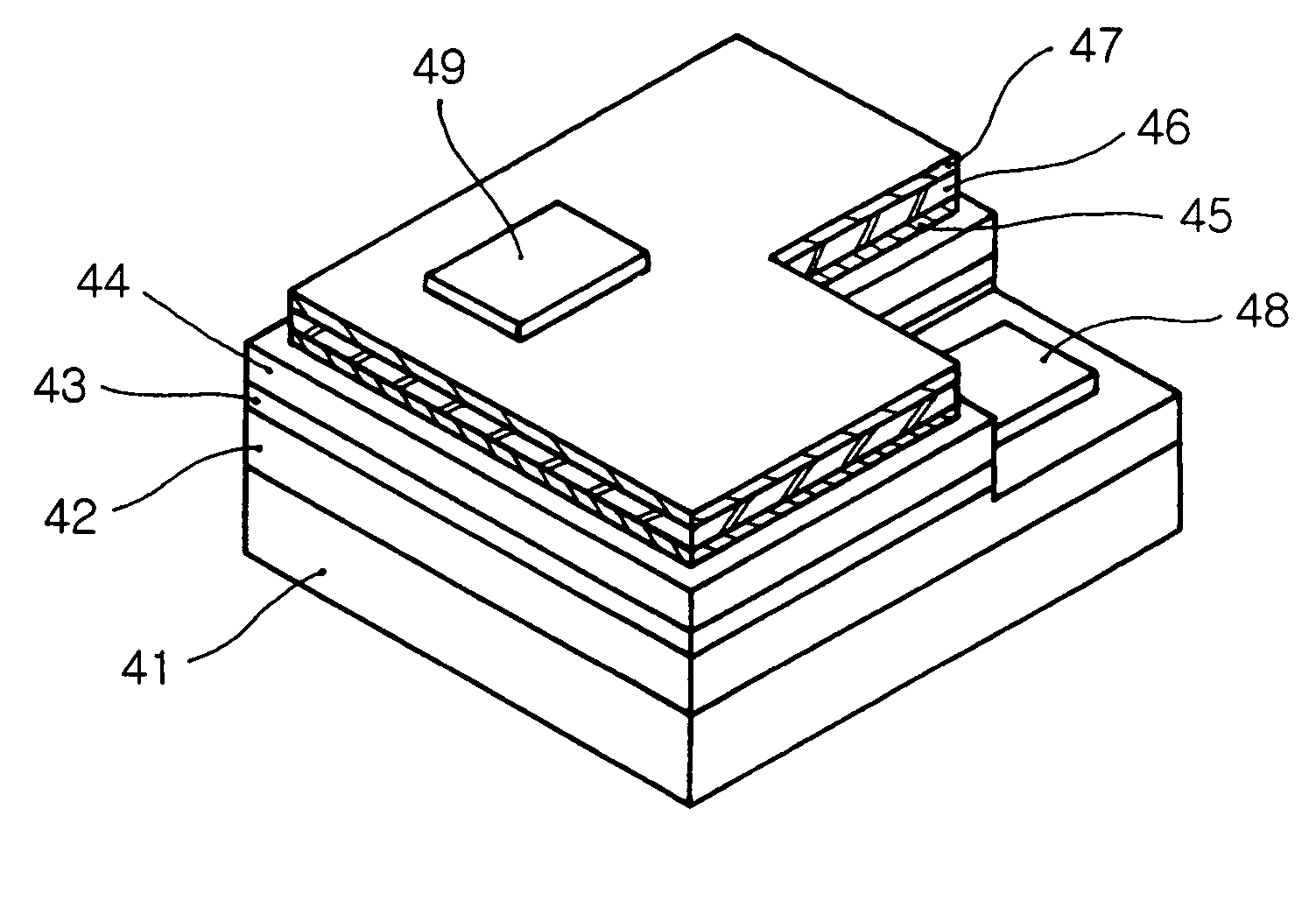
[0024]FIG. 3 is a sectional view illustrating a flip chip type nitride semiconductor light emitting device in accordance with the present invention. Referring to FIG. 3, the flip chip type nitride semiconductor light emitting device of the present invention comprises a substrate 31, an n-type nitride semiconductor layer 32 formed on the substrate 31, an active layer 33 formed on at least a part of the n-type nitride semiconductor layer 32, a p-type nitride semiconductor layer 34 formed on the active layer 33, a bonding force providing layer 35 which is formed on the p-type nitride semiconductor layer 34 and adapted to provide a bonding force relative to the p-type nitride semiconductor layer 34, a reflective electrode layer 36 which is formed on the bonding force providing layer 35 and adapted to reflect light produced in the ...


PUM


Abstract

Disclosed herein are a flip chip type nitride semiconductor light emitting device, which comprises a substrate for growing a nitride semiconductor material, an n-type nitride semiconductor layer formed on the substrate, an active layer formed on at least a part of the n-type nitride semiconductor layer, a p-type nitride semiconductor layer formed on the active layer, a bonding force providing layer formed on the p-type nitride semiconductor layer and adapted to provide a bonding force relative to the p-type nitride semiconductor layer, a reflective electrode layer formed on the bonding force providing layer, and adapted to reflect light produced in the active layer toward the substrate and to diffuse electric current, and a cap layer formed on the reflective electrode layer, and adapted to provide a bonding force between the reflective electrode layer and a bonding metal and to reduce contact resistance.

Description

BACKGROUND OF THE INVENTION[0001]1. Field of the Invention[0002]The present invention relates to a nitride semiconductor light emitting device and a manufacturing method thereof, and more particularly to a flip chip type nitride semiconductor light emitting device and its manufacturing method wherein a p-metal layer of the nitride semiconductor light emitting device, which has a flip chip structure, comprises three layers, namely, a bonding force providing layer, a reflective electrode layer, and a cap layer, so as to enhance a bonding force between the p-metal layer and a p-type nitride semiconductor layer of the device, to improve efficiencies of reflection and electric current diffusion, and to reduce contact resistance, resulting in enhanced brightness and driving voltage qualities of the device.[0003]2. Description of the Related Art[0004]Currently, in order to enable such a nitride semiconductor light emitting device to be utilized as a next-generation lighting apparatus, ther...

Claims


Application Information

Patent Timeline
Patent Type & Authority Patents(United States)
IPC IPC(8): H01L33/00H01L21/28H01L33/10H01L33/32H01L33/38H01L33/40H01L33/62
CPCH01L33/405H01L33/32
Inventor KIM, HYUN KYUNGKIM, YONG CHUNSHIN, HYOUN SOO
Owner SAMSUNG ELECTRONICS CO LTD
Why Eureka
Try Eureka