Memory circuit
a memory circuit and memory technology, applied in the field of memory circuits, can solve the problems of data error (bit error) locality, soft error, data error may be called soft error,
- Summary
- Abstract
- Description
- Claims
- Application Information
AI Technical Summary
Benefits of technology
Problems solved by technology
Method used
Image
Examples
embodiment 1
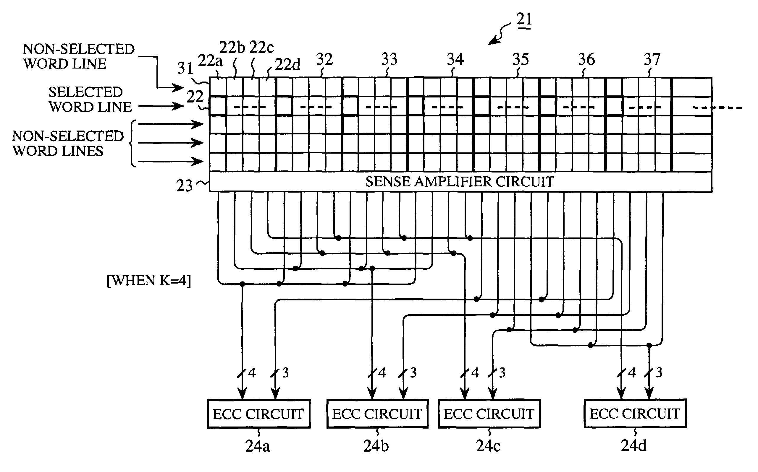
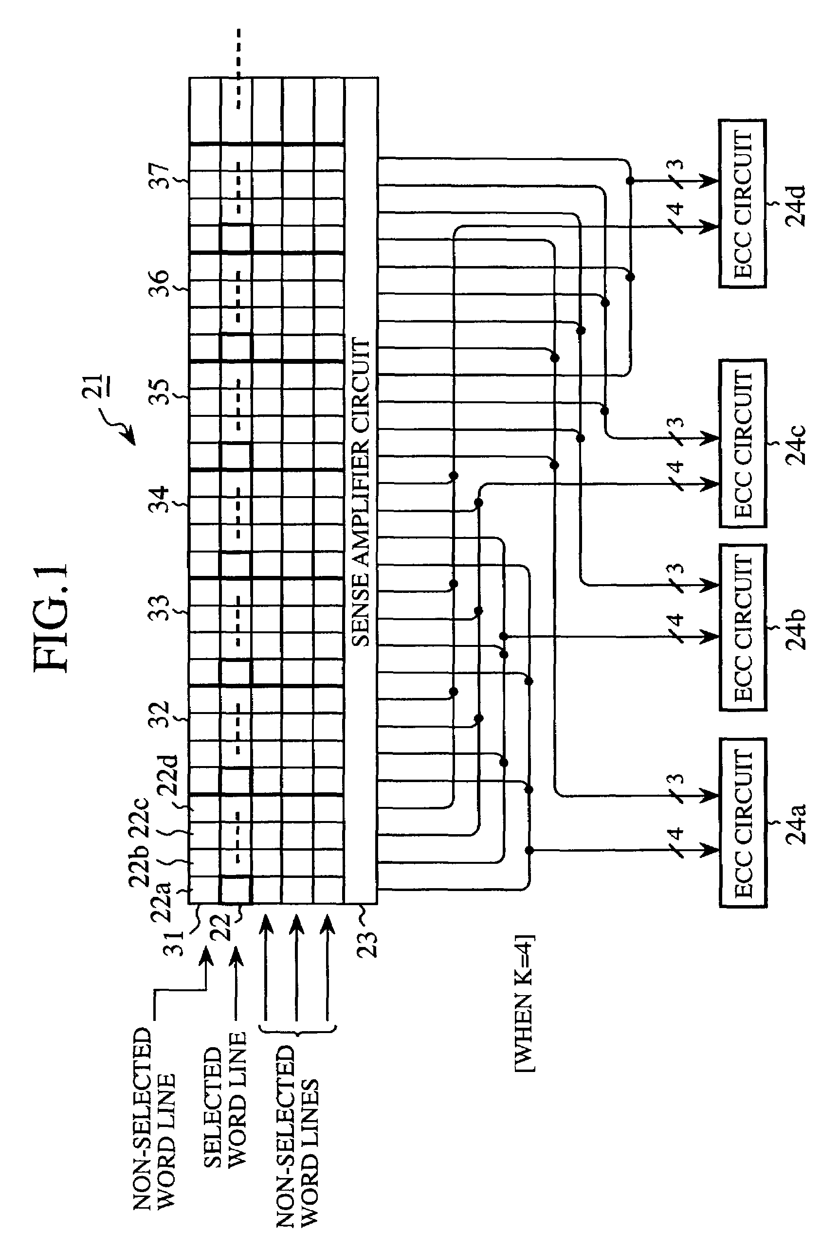
[0031]In FIG. 1, a reference numeral 21 represents a memory cell array. A reference numeral 22 represents a memory cell. A reference numeral 23 represents a sense amplifier circuit. Reference numerals 24a to 24d represent ECC circuits, respectively (Each of the ECC circuits 24a to 24d serves as an error correcting section). Data of (m+n) bits are read from and written to the memory cell array 21. The data of (m+n) bits are obtained by adding parity bits of n bits to data of m bits. The memory cell array 21 is divided into K bits arranged along a direction of a word line, where K represents a positive integer which is not less than two. Each unit having the K bits arranged along the direction of the word line will be called a memory unit. Successive memory units of (m+n) form a memory block. In the example being illustrated, K=4, m=4, and n=3. Each of the memory units is divided into 4 bits. The successive seven memory units form one memory block.
[0032]In FIG. 1, the memory units are...
embodiment 2
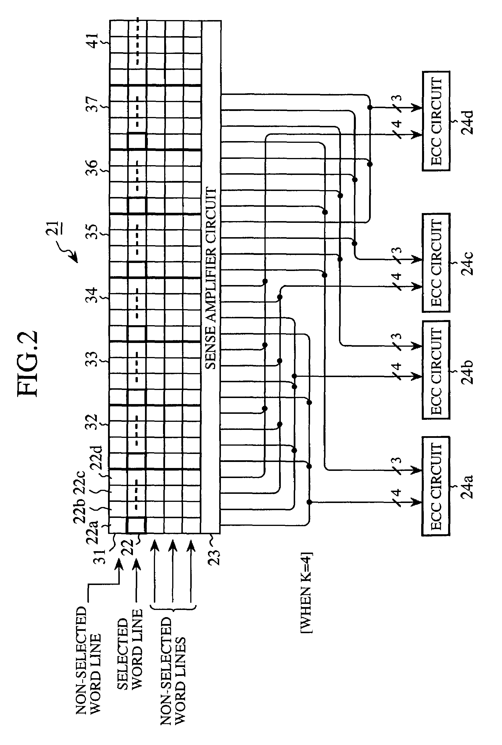
[0042]In FIG. 2, the same components as those of FIG. 1 are designated by the same reference numerals. A reference numeral 41 represents a spare memory unit (redundant memory unit). The spare memory unit 41 is similar in structure to each of the memory units 31 to 37. In other words, the spare memory unit 41 has memory cells 22 of 4 bits that are arranged along the word line. It will be assumed that a memory cell failure occurs in the memory unit 36 (for example, a defect based on manufacturing). The memory unit 36 is displaced with the spare memory unit 41. The first through the fourth rows 22a to 22d of the spare memory unit 41 are connected to the ECC circuits 24a to 24d, respectively.
[0043]A selection switch is used on displacing the memory unit 36 with the spare memory unit 41. More particularly, a laser repair fashion is used which sets the selection switch by a laser cutting. Although illustration is not made in FIG. 2, a laser repair fuse is cut so that a selector selects th...
embodiment 3
[0046]FIG. 4 shows a view for illustrating an example of a memory cell (SRAM cell) of an SRAM. T1 and T2 represent transistors, respectively. INT1 and INT2 represent inverters, respectively. A latch circuit is composed of the inverters INT1 and INT2 of two stages. A capacitance (including a parasitic capacitance) is given by Cs on a latch node. When each of the inverters INT1 and INT2 is supplied with a power voltage of Vcc, an accumulated charge is given by Cs×Vcc (coulombs).
[0047]When −Q (coulombs) represents a charge of an electron which generates on plunging the particle of the alpha ray or the neutron ray into the semiconductor substrate, the positive integer K′ which satisfies a relationship of K′>Q / (Cs×Vcc) is used as a division number.
[0048]The above-mentioned division number K′ represents a distance (worst value) between error bits which cause the memory circuit a data error, in case where the particle is plunged parallel to the word line. The multi-bit soft error hardly oc...
PUM
 Abstract
Description
Claims
Application Information


