Heat removal in SOI devices using a buried oxide layer/conductive layer combination

a technology of oxide layer and conductive layer, which is applied in the direction of semiconductor devices, basic electric elements, electrical equipment, etc., can solve the problems of increasing drain current, poor heat removal of devices on soi substrates, and significant disadvantages of soi devices, so as to improve heat transfer capabilities and improve quality and reliability.

Inactive Publication Date: 2007-07-03
GLOBALFOUNDRIES INC
View PDF7 Cites 24 Cited by
  • Summary
  • Abstract
  • Description
  • Claims
  • Application Information

AI Technical Summary

Benefits of technology

[0013]Due in part to the above methods, silicon-on-insulator substrates can be formed which have improved heat transfer capabilit

Problems solved by technology

This is because no connection is made to the channel region and charging of the floating body provides access towards a majority of carriers which dynamically lower the threshold voltage, resulting in increased drain current.
Although there are significant advantages associated with SOI technology, there are significant disadvantages as well.
For example, poor heat removal from devices on an SOI substrate is a significant disadvantage.
Electrical devices generate heat, and the inability to remove or dissipate the

Method used


Image

  • Heat removal in SOI devices using a buried oxide layer/conductive layer combination
  • Heat removal in SOI devices using a buried oxide layer/conductive layer combination
  • Heat removal in SOI devices using a buried oxide layer/conductive layer combination

Examples


Embodiment Construction

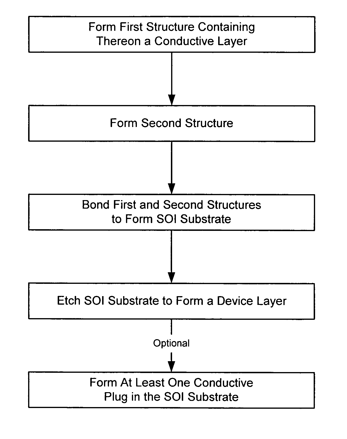
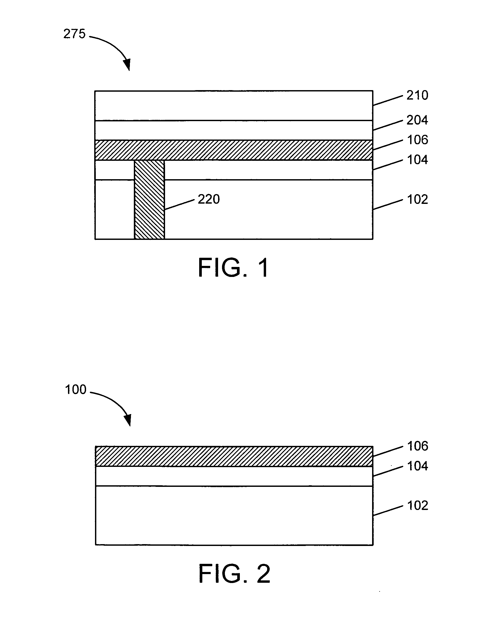
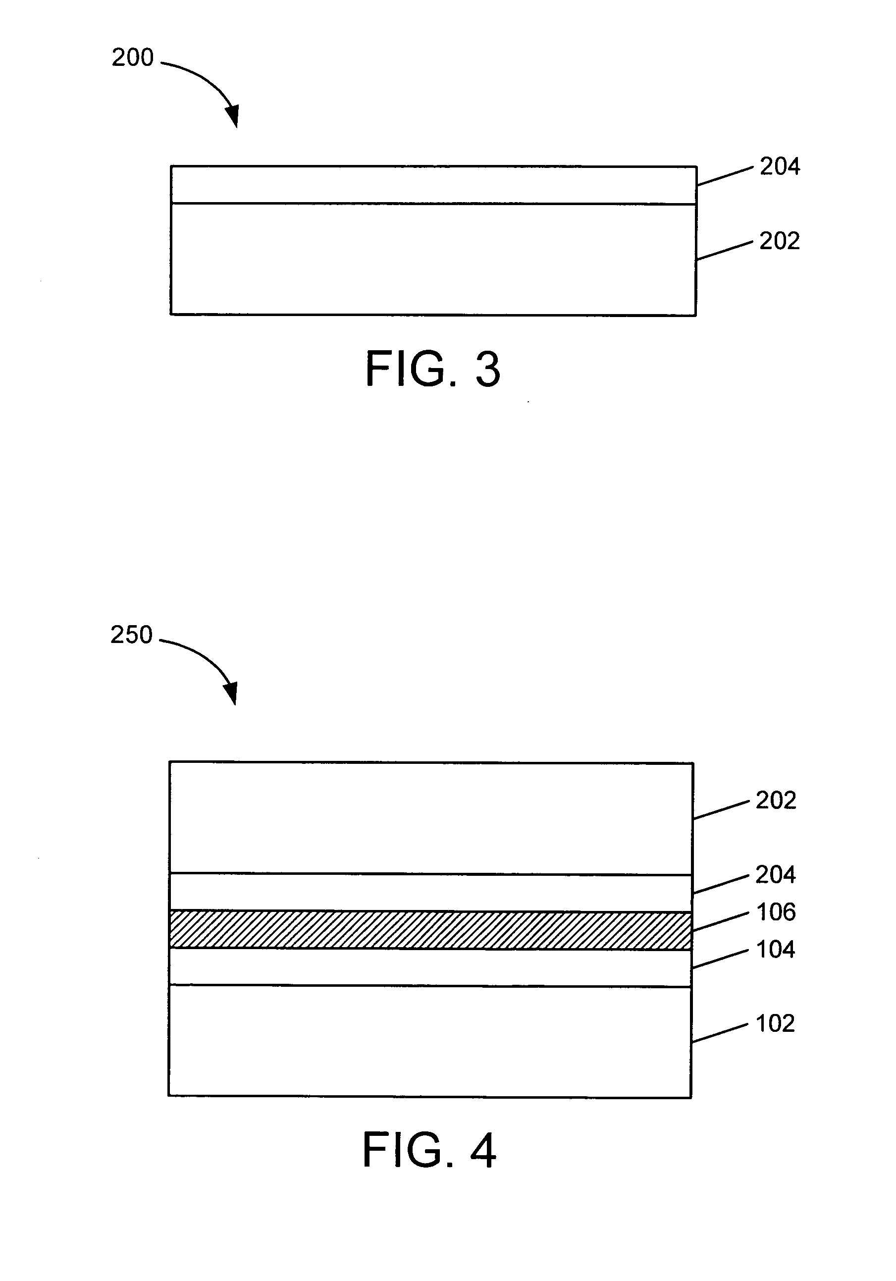
[0025]The present invention generally relates to improved Silicon-on-Insulator (SOI) devices. More particularly, the present invention relates to methods for removing heat from Silicon-on-Insulator devices and devices having such characteristics. As used throughout the specification and claims, the term conductive layer means a layer that is at least thermally conductive, and the term conductive plug means a plug that is at least thermally conductive. Such a layer and / or plug may, in some embodiments of the present invention, also be electrically conductive. Additionally, it should be noted that in the following text, range limits may be combined.

[0026]By forming an SOI substrate having improved heat removal characteristics, the performance of devices subsequently formed on the SOI substrate can be substantially improved. While not wishing to be bound to any theory, it is believed that by forming a conductive layer between two insulation layers (e.g., two buried oxide layers) accord...


PUM


Abstract

A method of forming a silicon-on-insulator substrate is disclosed, including providing a silicon substrate; depositing a first insulation layer over the silicon substrate; forming a conductive layer over the first insulation layer to a first structure; providing a second structure comprising a silicon device layer and a second insulation layer; bonding the first structure and the second structure together so that the conductive layer is located between the first and second insulation layers; and removing a portion of the silicon device layer thereby providing the silicon-on-insulator substrate having two discrete insulation layers. In one embodiment, the method further includes forming at least one conductive plug through the silicon substrate and the first insulation layer and/or the second insulation layer so as to contact the conductive layer. Methods of facilitating heat removal from the device layer are disclosed.

Description

RELATED APPLICATION DATA[0001]This application is a division of and claims priority under 35 U.S.C. §120 to commonly assigned U.S. application Ser. No. 10 / 174,328, filed Jun. 18, 2002, now U.S. Pat. No. 6,833,587, which in turn claims priority under 35 U.S.C. §119(e) to previously filed U.S. Provisional Application No. 60 / 298,980, filed on Jun. 18, 2001, entitled “Heat Removal in SOI Devices Using a Buried Oxide Layer / Conductive Layer Combination”, the disclosures of which are hereby incorporated herein by reference in their entirety.FIELD OF THE INVENTION[0002]The present invention generally relates to improved Silicon-on-Insulator (SOI) devices. More particularly, the present invention relates to methods for removing heat from Silicon-on-Insulator devices and devices having such characteristics.BACKGROUND OF THE INVENTION[0003]Silicon-on-Insulator (SOI) technology is of growing importance in the field of integrated circuits. SOI technology involves forming transistors in a relativ...

Claims


Application Information

Patent Timeline
IPC IPC(8): H01L21/84H01L21/762H01L27/01H01L27/12H01L31/0392
CPCH01L21/76256H01L21/84Y10S438/928
Inventor LIN, MING-REN
Owner GLOBALFOUNDRIES INC
Why Eureka
Try Eureka