Bonding structure of device packaging

a technology of device packaging and bonding structure, which is applied in the direction of transportation and packaging, coatings, chemistry apparatuses and processes, etc., can solve the problems of bridging phenomena, significant difference in device thermal expansion coefficient between adhesive agent and substrate, and likely generation of thermal stress deformation, so as to reduce the required bonding temperature, increase the bonding density, and increase the effect of fabrication reliability

Inactive Publication Date: 2007-07-03
IND TECH RES INST
View PDF17 Cites 5 Cited by
  • Summary
  • Abstract
  • Description
  • Claims
  • Application Information

AI Technical Summary

Benefits of technology

[0010]The disclosed bonding structure of device packaging mainly contains a first substrate and a second substrate. A surface of the first substrate has several metal pads and a first bonding metal layer. A surface of the second substrate has several electrodes and a second bonding metal layer. The first substrate is bonded with the second substrate. The first bonding metal layer and the second bonding metal layer are connected together. The metal pads and the electrodes are in electrical communications. In particular, the second substrate can be a flexible substrate, such as a polymer substrate, to buffer the stress produced by the bonding between the substrates.
[0012]The connection between the first and second bonding metal layers and the electrical connection between the electrodes can be accomplished by direct thermocompression, ultrasonic bonding, or surface activated bonding. They can be done by first activating the surfaces or undergoing ultrasonic oscillations, followed by the thermocompression. Processing the bonding interface with surface activation or ultrasonic oscillations can reduce the required bonding temperature, solving the high-temperature problem in existing bonding procedures.
[0013]The disclosed bonding structure of device packaging can be applied to the bonding between integrated circuit (IC) chips and substrates, without the need of NCF or ACF. In comparison with the prior art, the invention can increase the bonding density, achieve fine-pitch bonding, increase the fabrication reliability, reduce required steps, and lower the production cost.

Problems solved by technology

However, in the conventional flip-flop packaging method, the adhesive agent coated on the substrate has a serious difference in the coefficient of thermal expansion with respect to the device.
When the temperature changes, the thermal stress is likely generate deformation at the bumps between the device and the substrate.
The drawback of this technology, however, is that if the bonding pitch between adjacent metal bumps is very small, bridging phenomena will be happened.
Due to the pressure and heat, conductive particles have drifting motions to result in short circuiting between adjacent two conductive points.
Therefore, it cannot satisfy the requirement of miniaturization and the bonding density allows a pitch of 40 μm.
Its covalence bond constrains free electrons of the metal, making it hard to form metal bonds at the interface.
Therefore, it is not suitable for the applications in fine pitches.

Method used


Image

  • Bonding structure of device packaging
  • Bonding structure of device packaging
  • Bonding structure of device packaging

Examples


first embodiment

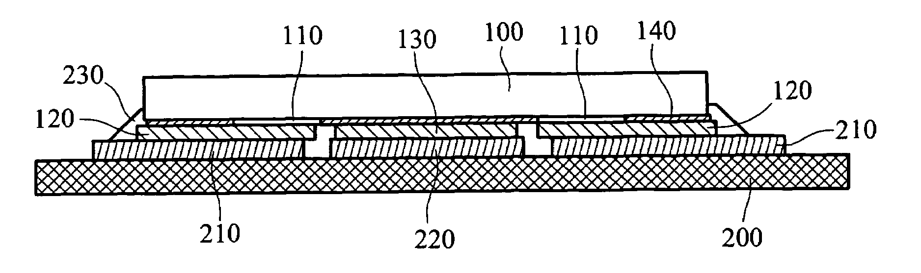
[0019]Please refer to FIG. 1 for a detailed description of the invention. As shown in the drawing, the invention contains a first substrate 100 and a second substrate 200. The first substrate 100 has several metal pads 110, adhesive metal circuit layers 120, a passivation layer 140, and a first bonding metal layer 130. In addition, the first substrate 100 has a first surface with a first center area, the several metal pads 110 are located on the first surface outside the first center area, and the first bonding metal layer 130 is located on the first center area. As can be seen in FIG. 1, the adhesive metal circuit layers 120 have a same height as that of the first bonding metal layer 130. Moreover, the adhesive metal circuit layers 120 have areas facing the second substrate and corresponding to the respective metal pads 110. The areas are larger than areas of the metal pads 110 confronting the adhesive metal circuit layers 120. The passivation layer 140 is formed on the surface of ...

second embodiment

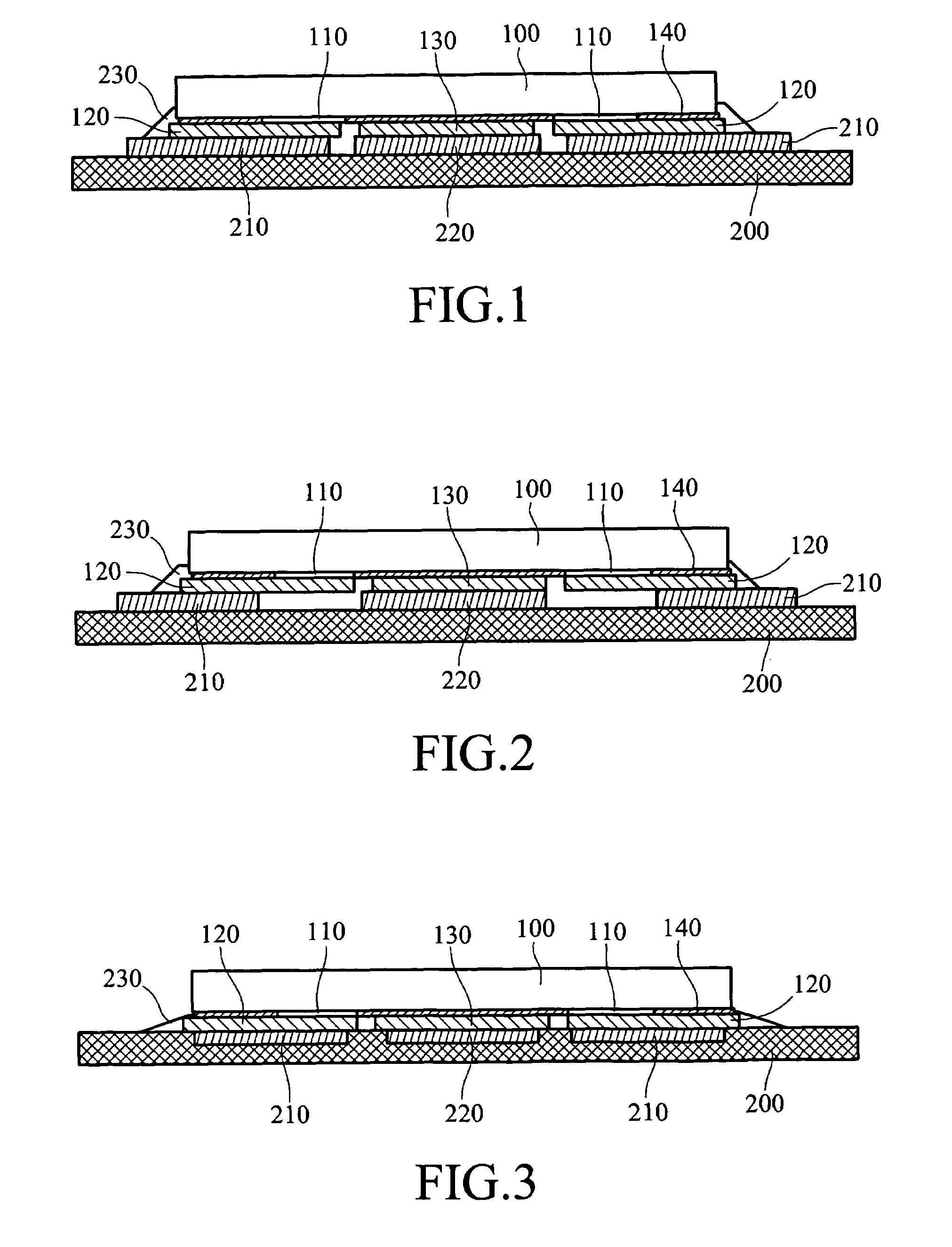
[0020]The metal pads on the first substrate are connected to the electrodes on the second substrate using the extension of the adhesive circuit on the first substrate. With reference to FIG. 2, the invention also contains a first substrate 100 and a second substrate 200. A surface of the first substrate 100 has several metal pads 110, an adhesive metal circuit 120, a passivation layer 140, and a first bonding metal layer 130. The passivation layer 140 is formed on the surface of the first substrate 110, exposing the metal pads 110. The adhesive metal circuit 120 is connected to the metal pads 110 and extends to cover the passivation layer 140. The first bonding metal layer 130 covers the passivation layer 140. A surface of the second substrate 200 has several electrodes 210 and a second bonding metal layer 220. The first substrate 100 is bonded with the second substrate 120 in such a way that the first bonding metal layer 130 is fixed onto the second bonding metal layer 220. The met...

third embodiment

[0021]Moreover, the invention can embed the electrodes 210 and the second bonding metal layer 220 into the second substrate 200, exposing only their top surfaces. A cross-sectional view of the third embodiment is shown in FIG. 3. It includes a first substrate 100 and a second substrate 200. The structure of the first substrate 100 is as described before. The electrodes 210 and the second bonding metal layer 220 installed on the surface of the second substrate 200 are embedded into the second substrate 200, exposing only their top surfaces. The first substrate 100 is bonded with the second substrate 200 surface to surface, so that the first bonding metal layer 130 is fixed onto the second bonding metal layer 220. The bonding border of the first and second substrates 100, 200 is filled with some adhesive agent 230. Using the embedded second substrate structure, the packaging volume can be further reduced.

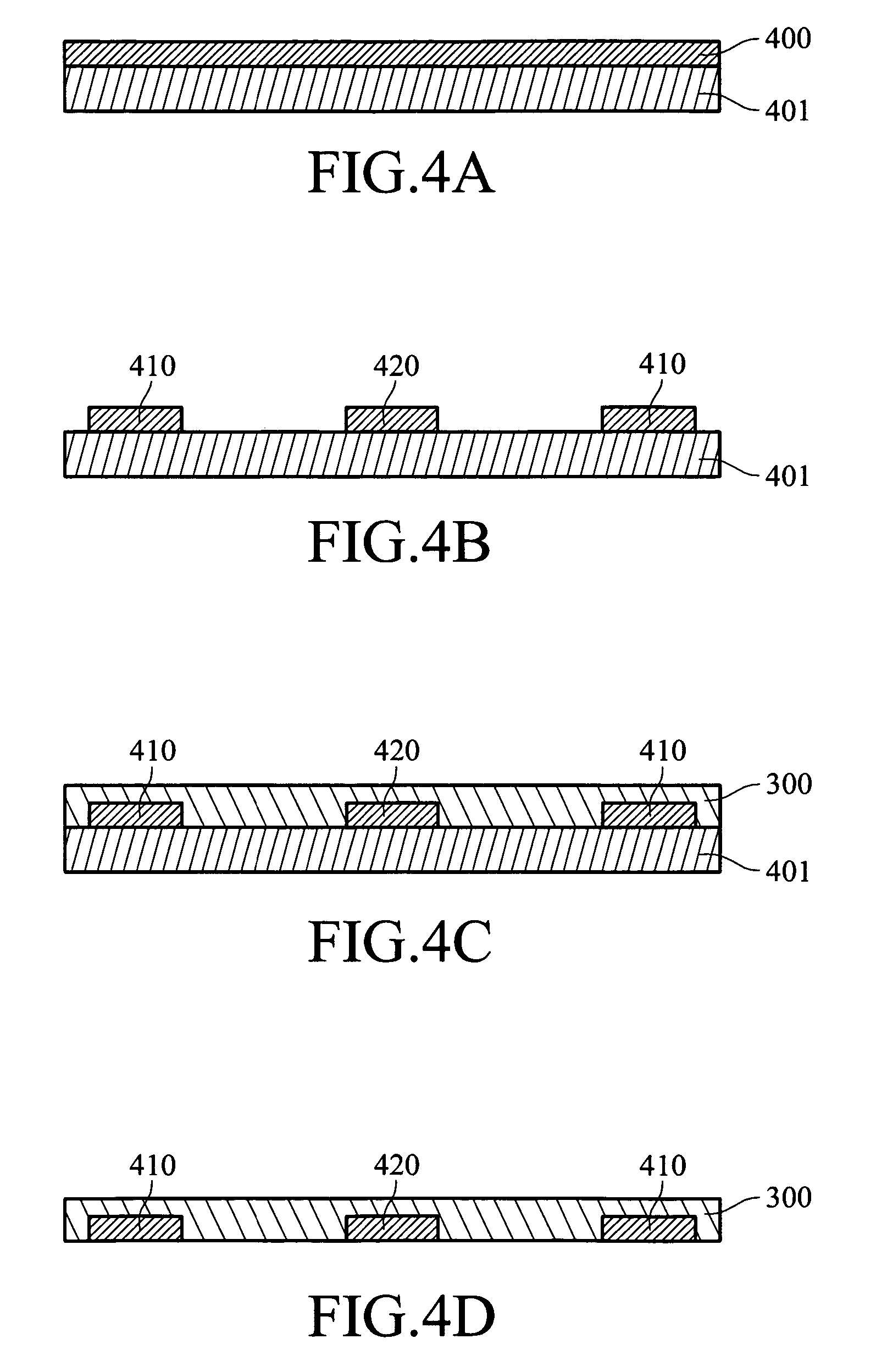
[0022]In particular, the embedded substrate can be prepared using the following s...


PUM

PropertyMeasurementUnit
areasaaaaaaaaaa
bonding structureaaaaaaaaaa
adhesiveaaaaaaaaaa

Abstract

A bonding structure of device packaging includes a first substrate and a second substrate. The surfaces of the first substrate have metal pads and a first bonding layer connected to the second substrate whose surfaces have a second bonding layer and electrodes. The first bonding layer is combined with the second bonding layer, and the metal pads are in electrical communications with the electrodes. The second substrate may be a flexible substrate to decrease the strain between the first substrate and the second substrate.

Description

BACKGROUND OF THE INVENTION[0001]1. Field of Invention[0002]The invention relates to a bonding structure and, in particular, to a bonding structure of device packaging.[0003]2. Related Art[0004]With the increasing requirements of the high device reliability, high bonding density, and device size reduction in semiconductor device packaging technology, conventional wire bonding is gradually replaced by the flip-chip technology.[0005]The flip-flop packaging technology is used to for pads or bumps at the junctions of a device and a substrate, in place of the lead frame used in the prior art, followed by coating a layer of an adhesive agent on the substrate surface. The structure is formed by directly embossing or welding the bumps of a device and the pads of a substrate together. In comparison with wire bonding, the prior art can reduce the transmission distance of electrical signals, which is suitable for the packaging of high-speed electronic devices. However, in the conventional flip...

Claims


Application Information

Patent Timeline
Patent Type & Authority Patents(United States)
IPC IPC(8): H01L23/48H01L21/56H01L21/60H01L23/498
CPCH01L24/81H05K3/328H01L21/563Y10T428/24917H01L2224/16H01L2224/81203H01L2224/81205H01L2224/81232H01L2224/81801H01L2224/81894H01L2224/83894H01L2924/01082H01L2924/14H05K3/20H05K3/321H05K3/325H05K2201/035H05K2201/10659H05K2201/10674H05K2203/0285H01L2924/01033H01L2224/81012H01L23/4985H01L2924/351H01L2924/00
Inventor LU, SU-TSAI
Owner IND TECH RES INST
Why Eureka
Try Eureka