Method for manufacturing a handling device and method for reversible bonding using such a device

a manufacturing method and technology of a handling device, applied in the manufacture of semiconductor/solid-state devices, solid-state devices, electric devices, etc., can solve the problems of deterioration of manufacturing steps, difficult to ensure a sufficient difference in adherence between the interfaces formed, and inability to generalize the method of reversible use, etc., to achieve the effect of facilitating the separation step

Active Publication Date: 2020-12-01
COMMISSARIAT A LENERGIE ATOMIQUE ET AUX ENERGIES ALTERNATIVES
View PDF7 Cites 4 Cited by
  • Summary
  • Abstract
  • Description
  • Claims
  • Application Information

AI Technical Summary

Benefits of technology

[0011]The invention offers a solution to the aforementioned problems. To do so, the invention firstly proposes a method for manufacturing in which a first wafer comprising a single adhesive layer is brought into contact with a second wafer comprising an antiadhesive layer. This bringing into contact makes it possible to obtain a handling device comprising a single adhesive layer comprising a single polymer layer having a low total thickness variation for low bonding temperatures without all the same requiring that the polymer of the adhesive layer has a low glass transition temperature.
[0012]By definition, the term adhesive is employed in the presence of one or more polymers which make it possible when they are arranged between two surfaces to increase the adherence energy between these two surfaces compared to the energy that would exist in its absence. Conversely, an antiadhesive decreases this adherence energy.
[0013]Moreover, the handling device obtained makes it possible to implement a method for reversible bonding of a wafer of interest to a handling device according to the invention not necessitating a step of cleaning of the wafer of interest or of recycling of the handling device at the end of the separation step.

Problems solved by technology

However, a single adhesive layer comprising a single polymer layer cannot in a general manner be employed in a method for reversible bonding and this applies even if the adherence is low at the level of the interfaces formed between the adhesive layer and the wafer of interest or the support wafer.
In fact, when the bonding is carried out by means of an adhesive layer comprising a single polymer layer, it is difficult to ensure a sufficient difference in adherence between the interfaces formed between the adhesive layer and the wafer of interest or the support wafer to be able to ensure dismantling.
However, when the step of bonding of the handling device with the wafer of interest is carried out at not very high temperatures, typically between 100 and 160° C. or even from room temperature to 160° C., the total thickness variation (TTV) of the adhesive layer becomes important and causes a deterioration of the manufacturing steps necessitating the use of a handling device. FIG. 1 illustrates the total thickness variation of a single adhesive layer composed of the adhesive 5150 of the Brewer Company for different bonding temperatures.
This low viscosity of the adhesive layer could bring about delaminatioris and make the use of a handling device incompatible with certain methods for manufacturing.
It will thus be understood from the preceding that, although it is possible to carry out a method for reversible bonding by means of a handling device with a single adhesive layer, it is currently very difficult to obtain a low total thickness variation for bonding temperatures typically between 100 and 160° C. or even from room temperature to 160° C. without resorting to a polymer having a low glass transition temperature and thus capable of bringing about a delamination during later steps carried out at higher temperatures.

Method used


Image

  • Method for manufacturing a handling device and method for reversible bonding using such a device
  • Method for manufacturing a handling device and method for reversible bonding using such a device
  • Method for manufacturing a handling device and method for reversible bonding using such a device

Examples


Embodiment Construction

[0046]Unless stated otherwise, a same element appearing in the different figures has a single reference.

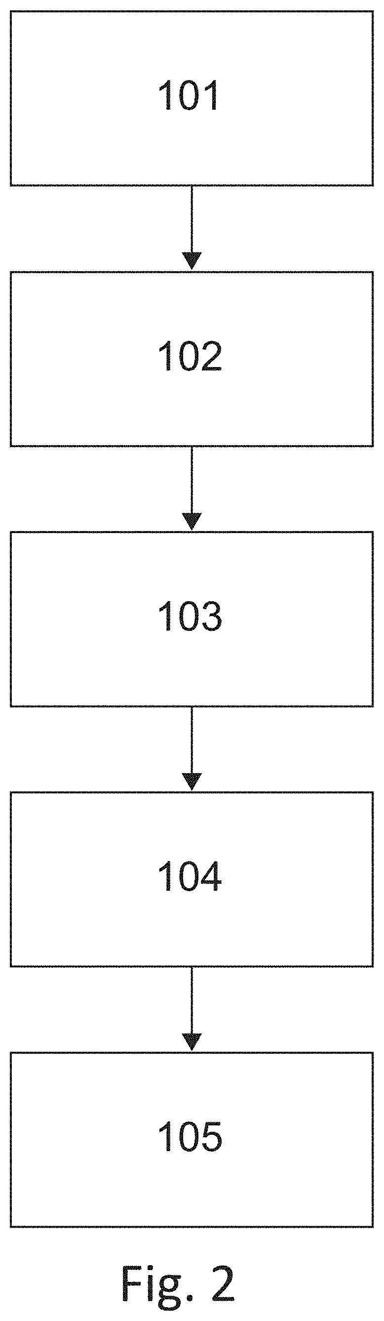
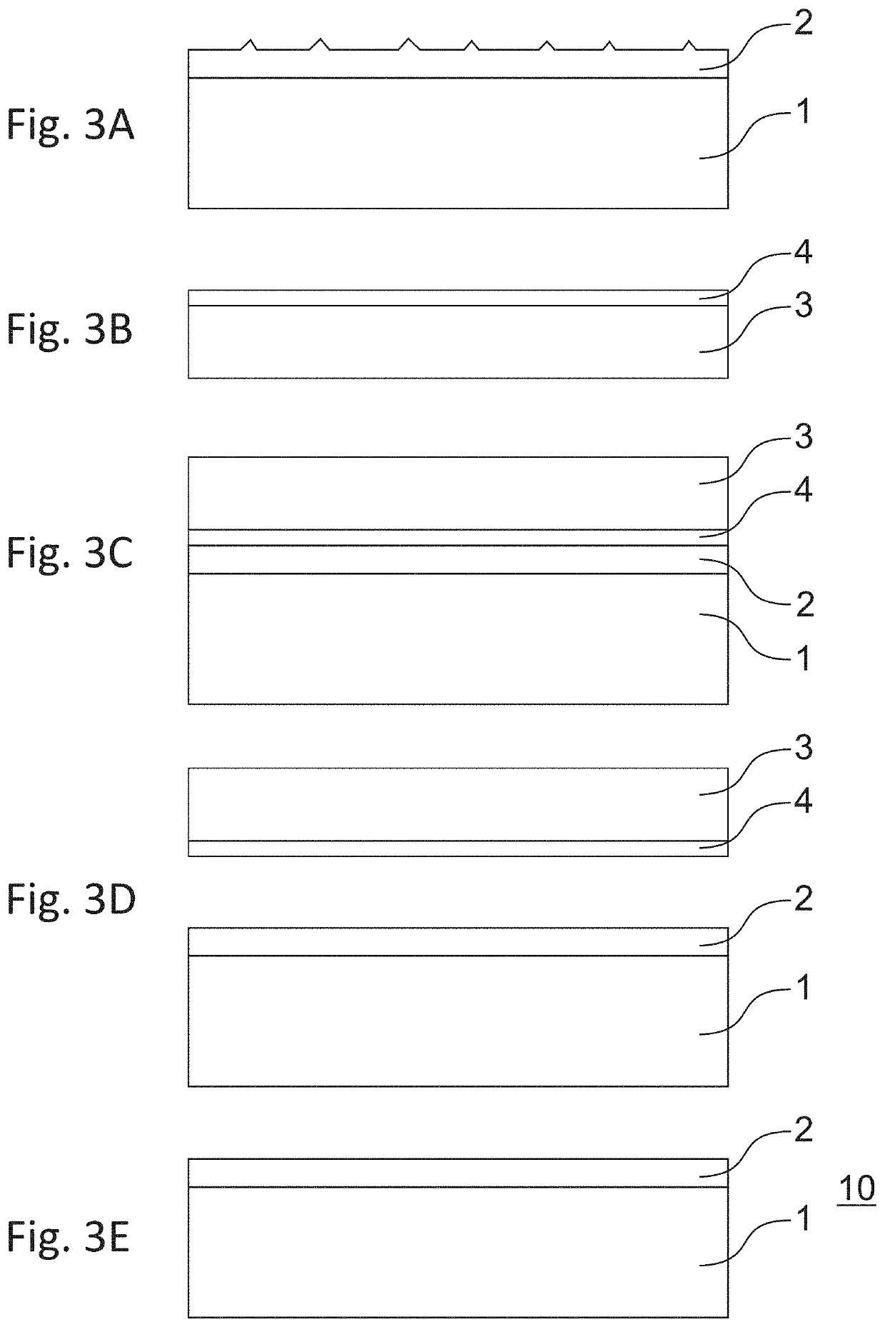
[0047]As illustrated in FIG. 2 and FIGS. 3A to 3E, a first aspect of the invention relates to a method for manufacturing a handling device 10. In one embodiment, the method according to the invention comprises:[0048]a step of deposition 101 (FIG. 2A) of a single adhesive layer 2 comprising a solvent on a first surface of a first wafer 1;[0049]a step of annealing 102 of the first wafer 1 so as to eliminate solvent from the single adhesive layer 2;[0050]a step of deposition 103 (FIG. 2B) of an antiadhesive layer 4 on a first surface of a second wafer 3 different from the first wafer 1;[0051]a step of bringing into contact 104 (FIG. 2C) the first wafer 1 and the second wafer 3, the bringing into contact taking place by the single adhesive layer 2 of the first wafer 1 and the antiadhesive layer 4 of the second wafer 3;[0052]a step of separation 105 (FIG. 2D) of the first wafer 1 and t...


PUM

PropertyMeasurementUnit
temperature Tcaaaaaaaaaa
temperature TCWaaaaaaaaaa
temperature Tcaaaaaaaaaa

Abstract

A method for manufacturing a handling device includes depositing a single layer of an adhesive on a first surface of a first wafer; depositing an antiadhesive layer on a first surface of a second wafer different from the first wafer; bringing into contact the first wafer and the second wafer, the bringing into contact taking place at the level of the single adhesive layer of the first wafer and the antiadhesive layer of the second wafer; separating the first wafer and the second wafer; the first wafer including the single adhesive layer forming a handling device. The bringing into contact of the first wafer and the second wafer is carried out at a temperature TC such that TC>Tg+100° C. where Tg is the glass transition temperature of the material composing the single adhesive layer of the first wafer.

Description

CROSS-REFERENCE TO RELATED APPLICATION[0001]This application claims priority to French Patent Application No. 1655076 filed Jun. 3, 2016, the entire contents of which is incorporated herein by reference in its entirety.TECHNICAL FIELD OF THE INVENTION[0002]The technical field of the invention is that of the manufacture of semiconductor devices. The present invention relates to the manufacture of a handling device, a handling device obtained by means of said method as well as a method for reversible bonding using said handling device.TECHNOLOGICAL BACKGROUND OF THE INVENTION[0003]When it is wished to carry out a manufacturing step on a wafer, hereafter called wafer of interest, it is known to bond this wafer of interest on a handling device, the latter being usually composed of a support wafer comprising an adhesive layer composed of one or more layers of polymers. The wafer of interest may for example be composed of a semiconductor material such as silicon. It may notably be a thinn...

Claims


Application Information

Patent Timeline
Patent Type & Authority Patents(United States)
IPC IPC(8): H01L21/683
CPCH01L21/6835H01L2221/68318H01L2221/68327H01L2221/68381H01L2221/6834
Inventor MONTMEAT, PIERREFOURNEL, FRANK
Owner COMMISSARIAT A LENERGIE ATOMIQUE ET AUX ENERGIES ALTERNATIVES
Why Eureka
Try Eureka