Semiconductor storage device

a technology of semiconductors and storage devices, applied in the direction of digital storage, electronic circuit testing, instruments, etc., can solve the problems of complex testing operations, and achieve the effect of improving testability

Inactive Publication Date: 2007-07-03
LONGITUDE LICENSING LTD
View PDF13 Cites 26 Cited by
  • Summary
  • Abstract
  • Description
  • Claims
  • Application Information

AI Technical Summary

Benefits of technology

[0019]Moreover, if the structure similar to that described above is to be implemented in a DRAM (dynamic random access memory) of the pre-fetch system (the system in which data is written in a register prior to writing data in a memory cell), it becomes necessary to provide a write bus, dedicated to the test mode, for re-writing the write data / expectation data each cycle, thus complicating the circuit structure.
[0021]It is therefore a principal object of the present invention to provide a semiconductor storage device in which it is possible to prevent the circuit from being increased in size and in which accommodation to a test with variable data may be facilitated to contribute to improved testability.

Problems solved by technology

The result is complex testing operations for tests like marching in which data are frequently changed.

Method used


Image

  • Semiconductor storage device
  • Semiconductor storage device
  • Semiconductor storage device

Examples


embodiments

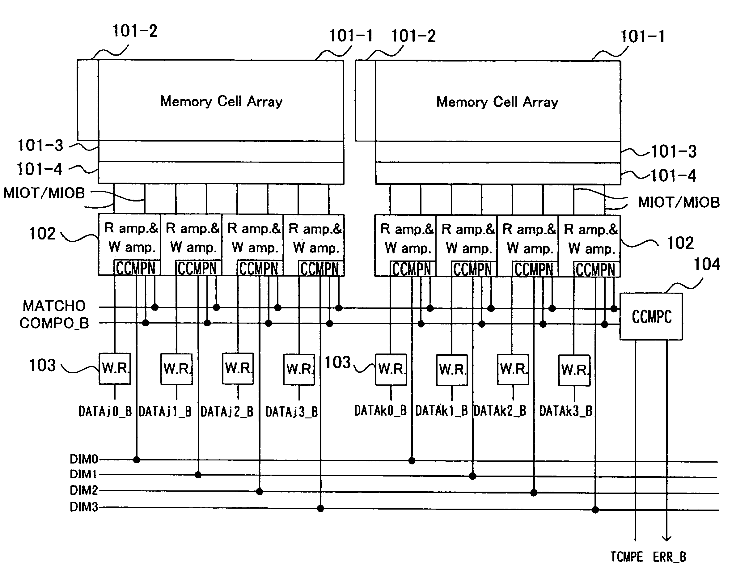
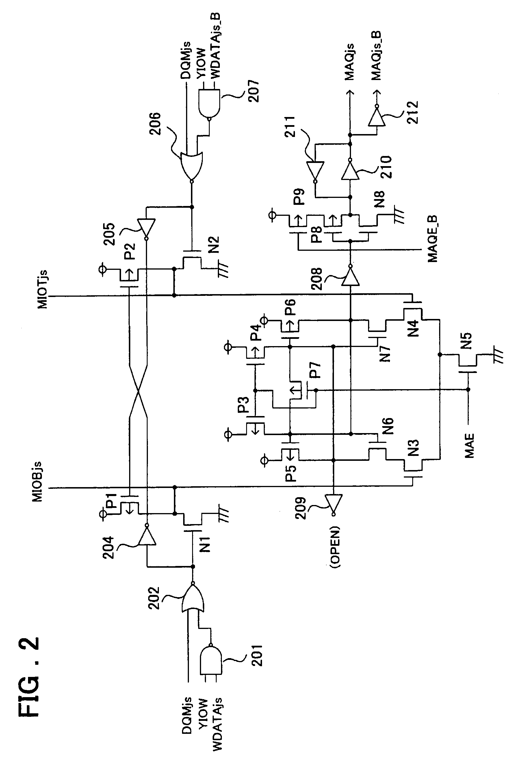
[0053]An embodiment of the present invention is now explained in further detail. FIG.1 is a schematic block diagram showing the structure of an embodiment of the present invention. The semiconductor storage device of the present embodiment has a pre-fetch function, such as an SDRAM (synchronous DRAM) or RDRAM (trademark of a product by Rambus Inc.) A write register for storage of pre-fetched data is used as a write register and as an expectation register for a parallel test, and the value of the write register is inverted and restored based on an inversion control signal from an external terminal. Referring to FIG.1, four write registers 103 and four read / write amplifiers (Ramp and Wamp) 102 are provided for a memory cell array 101-1, and each read / write amplifier (Ramp and Wamp) 102 is provided with a comparator (CCMPN) for comparing readout data and the expectation data to each other. Referring to FIG.1, the memory cell array 101-1 is provided with an X-decoder 101-2, supplied wit...


PUM


Abstract

A testing device for a semiconductor storage device suppresses the increase in the circuit size, provides for facilitated accommodation to a test with frequent changes in the test pattern, and improves testability of the semiconductor storage device. A plurality of holding circuits are provided holding write data for memory cells of a memory cell array. (Original) The write data from the holding circuits are written in the memory cells of the selected address. A plurality of comparators are supplied with data read out from the memory cells and with data held by the holding circuits as expectation data to compare the readout data and the expectation data. The non-inverted or inverted value of the write data held by the holding circuits is output as the write data to the memory cells and as expectation data to the comparators depending on the value of the inversion control signal.

Description

FIELD OF THE INVENTION[0001]This invention relates to a semiconductor storage device and, more particularly, to a semiconductor storage device convenient for parallel testing employing a testing device.BACKGROUND OF THE INVENTION[0002]As a parallel test, employing a testing device, a line mode test for semiconductor devices has become known (see for example the non-patent publication 1). First, the line mode test is briefly explained. FIG. 13 shows the structure of a semiconductor storage device disclosed in the non-patent publication 1. The storage device shown in FIG. 13 includes a multi-purpose register MPR (write / expectation value register) 1101 and a comparator circuit 1102 for complementary sub-IO lines SIO_T, SIO_B (bit line pair). The comparator circuit 1102 is formed by an Ex-OR circuit, and an output signal (coincidence detection signal) MATCH is wired-OR connected. The multi-purpose register MPR 1101, comprising a flip-flop formed by cross-connection of an output and an i...

Claims


Application Information

Patent Timeline
Patent Type & Authority Patents(United States)
IPC IPC(8): G01R31/28G11C11/401G11C29/26G11C29/34
CPCG11C29/26G11C2029/2602
Inventor YOSHIDA, HIROYASUOISHI, KANJI
Owner LONGITUDE LICENSING LTD
Why Eureka
Try Eureka