Semiconductor device

a technology of semiconductors and devices, applied in semiconductor/solid-state device testing/measurement, semiconductor devices, semiconductor/solid-state device details, etc., can solve problems such as gap discharge phenomenon, damage or breakdown of internal elements connected to bump electrodes, and discharge caused, so as to prevent discharge, increase connection strength, and suppress excessive accumulation of charge

Inactive Publication Date: 2007-07-10
NEC ELECTRONICS CORP
View PDF21 Cites 22 Cited by
  • Summary
  • Abstract
  • Description
  • Claims
  • Application Information

AI Technical Summary

Benefits of technology

[0021]It is the object of the present invention to provide an LSI which is capable of coping with the increase in the number of pins without increase in the chip size, and suppress excessive accumulation of charge to DBPs, even if it is equipped with the DBPs for increasing the connection strength or the like at mounting, and is capable of preventing discharge to adjacent bump electrodes (pins) and breakdown of the semiconductor chip due to stored charge (electrostatic noise).

Problems solved by technology

However, it became clear with the configuration of the semiconductor chip as disclosed in well-known examples 1 and 2 that when electrostatic noise is applied to the DBPs, there arises a problem in that discharge is caused between the neighboring bump electrodes, and the internal elements connected to the bump electrodes are damaged or broken down.
More specifically, when there exist externally connected electrodes, like the DBPs in this case, that are not connected to any of the elements within the semiconductor chip, and electrostatic noise is applied to the DBPs, it results in a gap discharge phenomenon due to absence of discharge route for the charge.
Since, however, the electrostatic noise due to the gap discharge phenomenon is a pulse steeper than the breakdown voltage of the electrostatic discharge protection circuit, there is a possibility that it breaks down the semiconductor chip.
The problem mentioned above is brought about because this value is gentle compared with the rise time of the discharge waveform in the gap discharge.
However, since the bonding pad 812 and the electrostatic discharge protection circuit 814 dedicated to the NC pin are formed in this method, the chip size becomes large as the number of the NC pins increases and the number of effective chips per semiconductor wafer decreases, so that it gives rise to the problem of increase in the production cost.
However, it is also necessary in this method to provide a resistor for each NC pin which requires the chip size to be increased, so that similar to the well-known example 3, the number of effective chips per semiconductor wafer, leading to the problem of increase in the production cost.
However, it will result in a problem that the lead-out of the wiring conductors connected to the bump electrodes for signals on the mounting substrate becomes difficult. FIG. 13 shows drawings for describing the problem, which consists of a plan view of the electrodes and a wiring pattern of a mounting substrate 900 to be connected to external connection bumps of an FCLSI 500 when, for example, the FCLSI 500 in FIG. 5 is mounted on the mounting substrate 900, and a schematic enlarged plan view of the portion corresponding to portion B of the FCLSI 500.
Accordingly, when the outermost peripheral electrode is a DBP connected to a fixed potential such as the ground potential, the number of signal lines that can be led out to the outside from the mounting region of the FCLSI 500 is reduced, so that the number of BPs for signal that can be available for input / output of signals among the bumps of the FCLSI 500 is reduced, which becomes an especially serious problem in a signal processing LSI or the like needed for a large number of signal terminals.
Furthermore, the problems related to the LSI or the semiconductor chip disclosed in the well-known example 1 or the well-known example 2 will become more serious because of the anticipation that the bump electrode space will be reduced further with a further advancement in miniaturization and increase in the pin number of the future LSIs.

Method used


Image

  • Semiconductor device
  • Semiconductor device
  • Semiconductor device

Examples


Embodiment Construction

[0038]Referring to the accompanying drawings, the present invention will now be described.

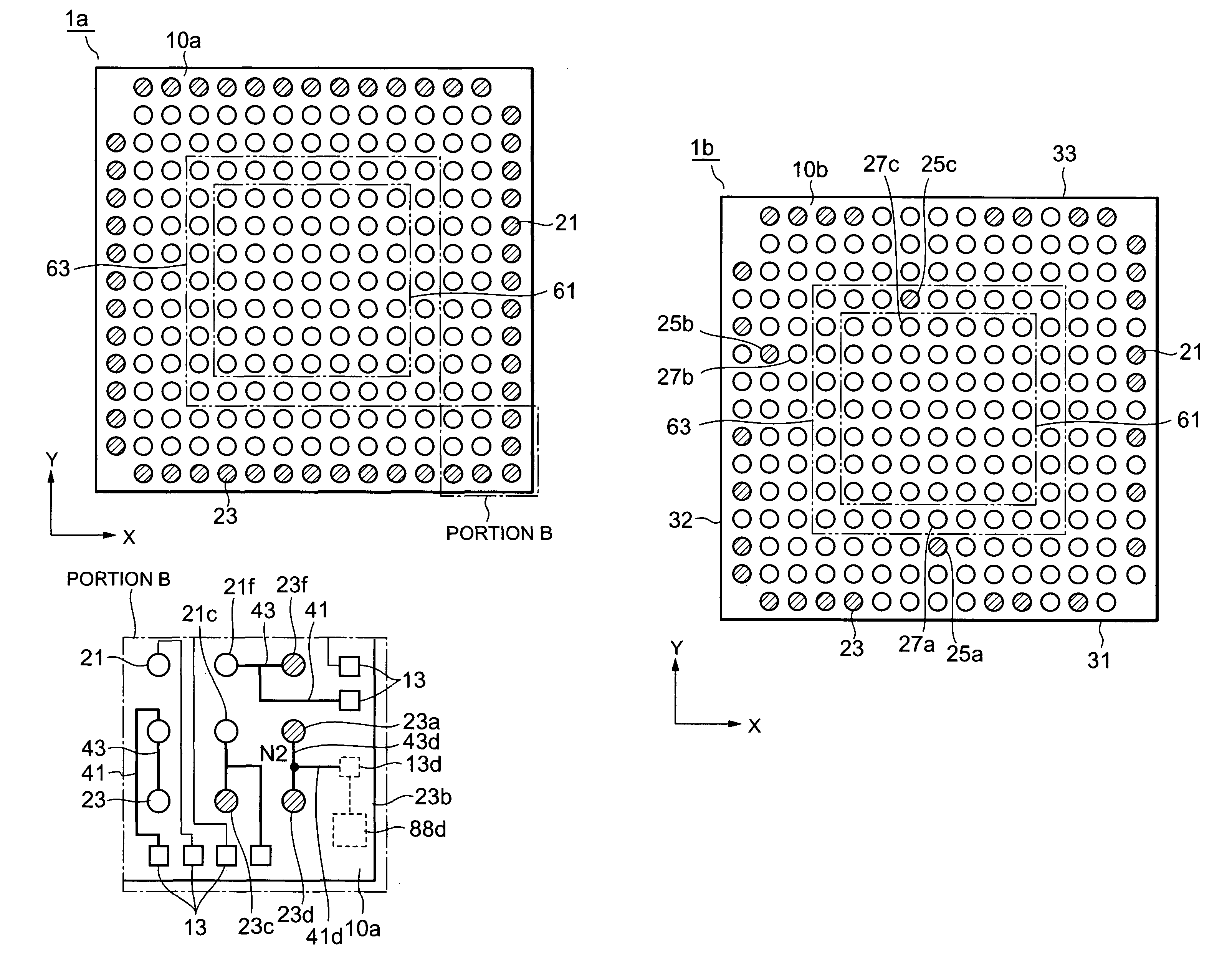
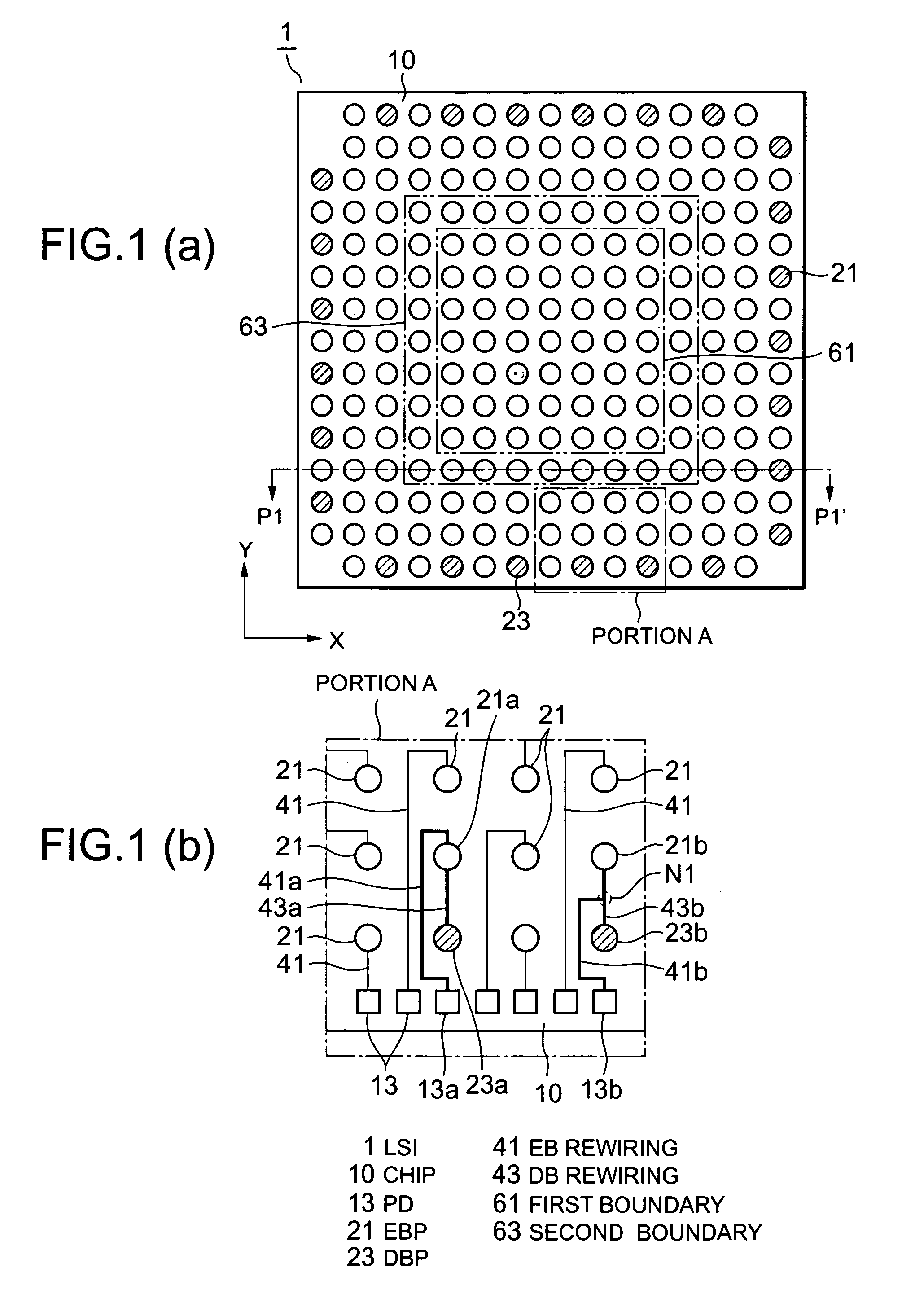
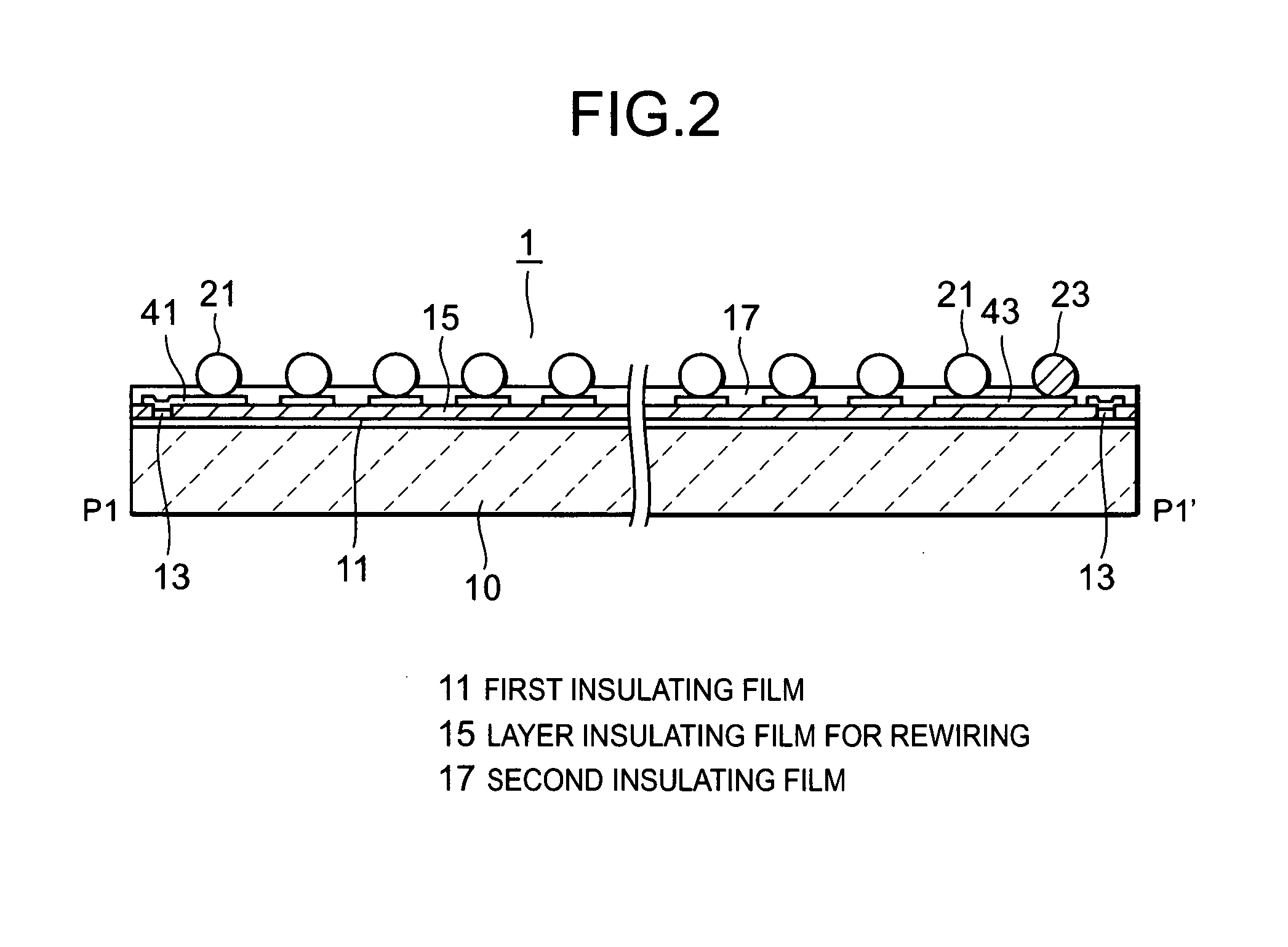
[0039]FIGS. 1a–1b are drawings showing an embodiment of the semiconductor device according to the present invention, where part (a) is a schematic plan view on the side of bump formation face of an FCLSI, and (b) is an enlarged plan view of portion A in part (a). FIG. 2 is a schematic sectional view along line P1–P1′ in FIG. 1(a). Moreover, FIGS. 3a–bb shows schematic drawings of an example of the semiconductor chip forming the FCLSI, where part (a) and part (b) are respectively examples of a plan view showing the internal constitution of the chip and an electrostatic protection circuit.

[0040]Referring to FIG. 1 to FIG. 3, an LSI 1 of this embodiment is equipped, on the side of element formation face of a semiconductor chip 10 where external connection pads (referred to as PDs hereinafter) 13 being chip electrodes are formed on desired elements, wirings (neither are shown) and a first insulatin...


PUM


Abstract

The present invention provides a large scale integrated circuit which is capable of coping with the problems associated with the situation in which the number of pins used in the circuit is increased, and is capable, even when dummy bumps (DBPs) are installed, of suppressing storage of an excessive charge to the DBPs and prevent discharge to adjacent bump electrodes and prevent breakdown of a semiconductor chip due to electrostatic noise. On the element formation face of the semiconductor chip wherepads (PDs) are formed, a layer insulating film for rewiring, external bumps (EBPs) that correspond respectively to PDs formed on the layer insulating film, dummy bumps (DBPs) lacking corresponding PDs on the semiconductor chip, external bump rewirings that connect the PDs and the corresponding EBPs, and dummy bump rewirings that connect DBPs and prescribed EBPs are formed in addition. An electrostatic protection means is installed between a PD connected to an EBP that is connected to a DBP and an internal circuit section or an I/O circuit section of the semiconductor chip.

Description

BACKGROUND OF THE INVENTION[0001]1. Field of the Invention[0002]The present invention relates to a semiconductor device which uses bumps formed of solder balls or the like as external connection terminals, and more particularly to a semiconductor device that is enhanced in the breakdown voltage to electrostatic noise.[0003]2. Description of the Prior Art[0004]In the semiconductor devices (referred to as LSIs hereinafter) of recent years, the increase in the number of pins used is remarkable along with the achieved high level of integration and scale, as a result of advancement in the micro processing technology. As the methods of making the increase in the number of pins and miniaturization of the LSIs compatible, flip chip type LSIs (referred to as FCLSIs hereinafter), CSP (chip size package / chip scale package) type LSIs, and the like, in which bumps for external connection are formed two-dimensionally on the main face side where semiconductor chip elements are formed via an insula...

Claims


Application Information

Patent Timeline
Patent Type & Authority Patents(United States)
IPC IPC(8): H01L23/48H01L23/12H01L21/60H01L23/498H01L23/50H01L23/58H01L23/60
CPCH01L22/32H01L23/49816H01L23/49838H01L23/50H01L24/06H01L2924/1306H01L2224/48091H01L2924/12041H01L2924/01033H01L2924/01024H01L2924/01023H01L2924/01005H01L2224/73265H01L2224/32225H01L2224/16225H01L24/48H01L2924/15311H01L2924/15173H01L2924/14H01L2224/0401H01L2224/48227H01L2924/01004H01L2924/01006H01L2924/01013H01L2924/01014H01L2924/01029H01L2924/01039H01L2924/01046H01L2924/01078H01L2924/01079H01L2924/01082H01L2924/014H01L2924/00012H01L2924/00014H01L2924/00H01L24/45H01L24/73H01L2224/05554H01L2224/451H01L2224/45144H01L2924/10162H01L2924/181H01L2924/351
Inventor UEDA, YOSHITAKA
Owner NEC ELECTRONICS CORP
Why Eureka
Try Eureka