
Pulse polarity modulation circuit

a polarity modulation and pulse technology, applied in pulse manipulation, pulse frequency/rate modulation, pulse technique, etc., can solve the problems of large noise, difficulty in realizing low power consumption and space saving, etc., and achieve the effect of reducing noise and low power consumption

Inactive Publication Date: 2007-07-10
FUJITSU LTD
View PDF6 Cites 6 Cited by
  • Summary
  • Abstract
  • Description
  • Claims
  • Application Information

AI Technical Summary

Benefits of technology

The present invention provides a pulse polarity modulation circuit that can achieve low power consumption, miniaturization, and reduce noise at a middle level. The circuit uses differential transistor pairs that are double stacked and coupled together, allowing for a more efficient and compact design. The circuit also includes a single pulse generator, which further reduces power consumption and noise. Overall, the invention improves the performance of ultrafast pulse communications systems by effectively suppressing noise and amplifier noise.

Problems solved by technology

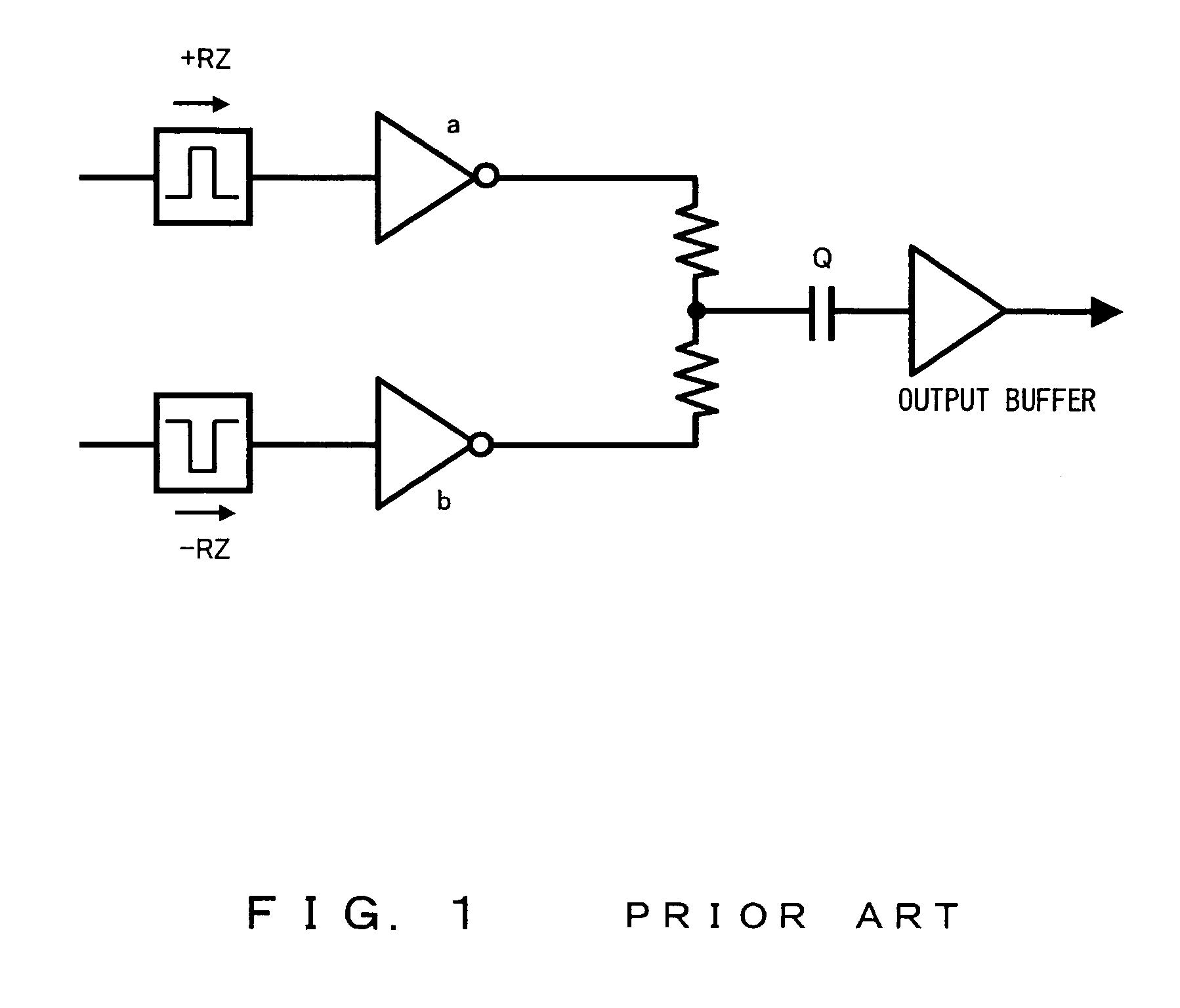
In the converter of patent document 1, however, there is a problem that it is difficult to realize low power consumption and space saving because dual-circuit pulse generators are required.
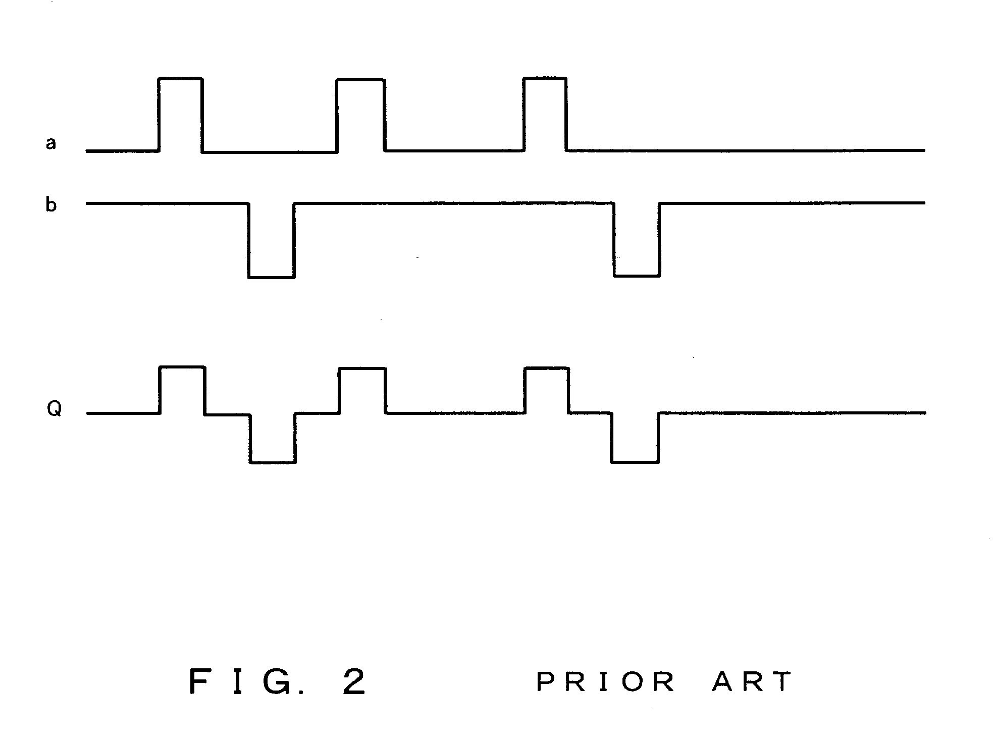
Further, as a pulse circuit for ultra-wide-band communication, it is desirable to use the differential circuit as described; however, the gain of the differential circuit attains a maximum around a logic threshold value which is the logic mid-point (0 point); therefore, if minute noise occurs around the middle level, there is a problem that the noise is amplified to a large degree by an amplifier circuit generally placed at a subsequent stage, and additional circuit design is required to keep the middle level flat.

Method used


Image

  • Pulse polarity modulation circuit
  • Pulse polarity modulation circuit
  • Pulse polarity modulation circuit

Examples


Embodiment Construction

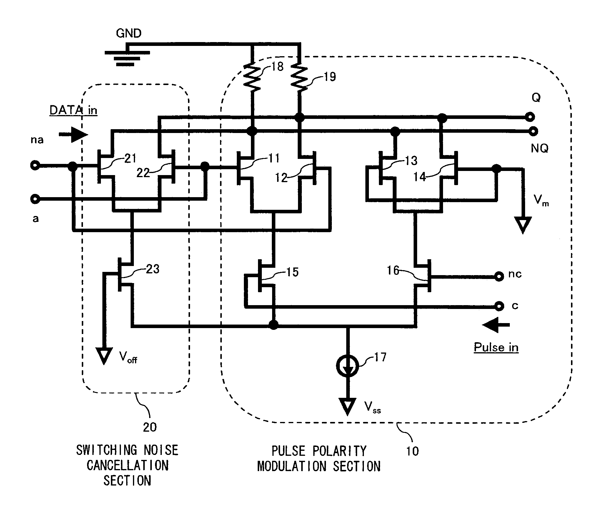
[0025]FIG. 3 is the principle block diagram of a pulse polarity modulation circuit according to the present invention. FIG. 3 shows the principle structure of the pulse polarity modulation circuit in which differential transistor pairs are double stacked and two transistors constituting a differential transistor pair 1 in a lower stage are coupled to their respective differential transistor pairs 2 and 3 in an upper stage.

[0026]In the pulse polarity modulation circuit according to the present invention, one of the differential transistor pairs in the upper stage, that is, the differential transistor pair 2 outputs polarity modulation pulses. The gates of the other differential transistor pair, that is, the differential transistor pair 3, are coupled together, and a middle potential between logic high and low is applied to the gates

[0027]Thus, in the pulse polarity modulation circuit according to the present invention, by applying the logic middle potential to the gates of the differ...


PUM


Abstract

In order to provide a high-speed-pulse polarity modulation circuit for realizing low power consumption and miniaturization and reducing noise occurring at a middle level which is a baseline for a bipolar pulse, a modulation circuit for converting a unipolar pulse into a bipolar pulse in accordance with a value of input data is structured such that differential transistor pairs are double stacked, and one of the differential transistor pairs in an upper stage outputs polarity modulation pulses, and a middle potential between logic high and low is applied to the gates of the other differential transistor pair the gates of which are coupled together.

Description

CROSS-REFERENCE TO RELATED APPLICATIONS[0001]This application is based upon and claims the benefit of priority from the prior Japanese Patent Application No. 2004-346935 filed on Nov. 30, 2004, the entire contents of which are incorporated herein by reference.BACKGROUND OF THE INVENTION[0002]1. Field of the Invention[0003]The present invention relates to an ultrafast integrated circuit used for ultra-wide-band communications for example and a technique of generating an ultrashort pulse required for the communications, and more particularly, to a pulse polarity modulation circuit for converting a unipolar pulse into a bipolar pulse.[0004]2. Description of the Related Art[0005]There is a general requirement in many communication devices, to convert a unipolar signal into a bipolar signal. It is desirable for this kind of unipolar / bipolar converter to be as small as possible and have low power consumption and a low-noise characteristic.[0006]Particularly, in ultra-wide-band communicati...

Claims


Application Information

Patent Timeline
Patent Type & Authority Patents(United States)
IPC IPC(8): H03K7/00
CPCH03M5/18
Inventor KAWANO, YOICHI
Owner FUJITSU LTD
Learn More