Storage apparatus and semiconductor apparatus

a technology of storage apparatus and semiconductor, applied in the direction of static storage, digital storage, instruments, etc., can solve the problems of power consumption, limited number of times of writing, slow reading speed, etc., and achieve the effect of stable recording and shortening the time required for recording

Active Publication Date: 2007-07-10
SONY SEMICON SOLUTIONS CORP
View PDF4 Cites 20 Cited by
  • Summary
  • Abstract
  • Description
  • Claims
  • Application Information

AI Technical Summary

Benefits of technology

[0032]The present invention is to be achieved in light of the above-described issues, and there is a need for providing a storage apparatus and a semiconductor apparatus which enables stable recording, and can shorten the time required for recording of information, while realizing writing and erasing.
[0034]Here, a common potential applied to the terminal of each of the memory devices is set to the intermediate potential which is a predetermined potential within a range from the ground potential to the power supply potential (not including the ground potential and the power supply potential), which enables the writing and erasing of the storage element.
[0035]More specifically, the intermediate potential is set within a range in which the application of the electric signal not lower than the first threshold signal to the storage element allows a resistance value of the storage element to change from a high state to a low state, thereby enabling the writing into the storage element. Also, the intermediate potential is set within a range in which the storage element which has come into the low resistance value state by applying the electric signal not lower than the first threshold signal can shift from the low resistance value state to the high resistance value state, thereby enabling the erasing of the storage element. Namely, the intermediate potential is set to a range in which the application of the electric signal not lower than the first threshold signal to the storage element allows the resistance value of the storage element to change from the high state to the low state, and at the same time, the storage element which has come into the low resistance value state by applying the electric signal not lower than the first threshold signal can shift from the low resistance value state to the high resistance value state, thereby enabling the writing and erasing of the storage element.
[0037]Furthermore, the storage element is structured in such a manner that a storage layer is sandwiched by a first electrode and a second electrode, and the application of the electric signal not lower than the first threshold signal between the first electrode and the second electrode allows the storage element to shift from the high resistance value state to the low resistance value state, and the application of the electric signal not lower than the second threshold signal between the first electrode and the second electrode allows the store element to shift from the lower resistance value state to the high resistance value state.
[0039]Here, the provision of the potential supply means for applying the intermediate potential as the common potential to the terminal of each of the memory devices enables the writing and erasing of the storage element.
[0040]In the above-described storage apparatus and the semiconductor apparatus of the present invention, stable recording of information can be performed, and the time required for recording the information can be shortened, while the writing and erasing are realized.

Problems solved by technology

However, since DRAM is volatile memory, which loses information upon turning off power, nonvolatile memory, which holds information after turning off power, has been desired.
Furthermore, it is considered that in the case of the above-mentioned memories, their non-volatility can make refreshing operation unnecessary and reduce power consumption.
However, at present, it is difficult for FeRAM to perform nondestructive reading and since it performs destructive reading, the reading speed is slow.
Furthermore, since polarization reversal according to reading or recording is limited in number of times, writing is limited in number of times.
Furthermore, since MRAM needs a magnetic field for recording, and a current flowing through wiring generates the magnetic field, a large amount of current is necessary in recording.
Since this phase change memory performs switching by using temperature, there is an issue that it is sensitive to changes in environmental temperature.
Accordingly, PMC disadvantageously cannot endure high temperatures in a step of manufacturing a storage element, for example, in a step of forming a CVD insulating film, a protecting film or the like.
Moreover, since both of the materials of the storage layers proposed in the constitutions of RRAM's described in Non-Patent Document 1 and Non-Patent Document 2 are crystalline, RRAM has problems that thermal processing at about 600° C. is necessary, that it is extremely difficult to manufacture monocrystal of the proposed materials, that miniaturization is difficult because the use of polycrystal brings about the influence of grain boundary, etc.
Therefore, it is difficult to perform stable recording.
The above-described processes makes the time required for recording longer, and thus makes it difficult to overwrite data or the like at a high speed.

Method used


Image

  • Storage apparatus and semiconductor apparatus
  • Storage apparatus and semiconductor apparatus
  • Storage apparatus and semiconductor apparatus

Examples


example

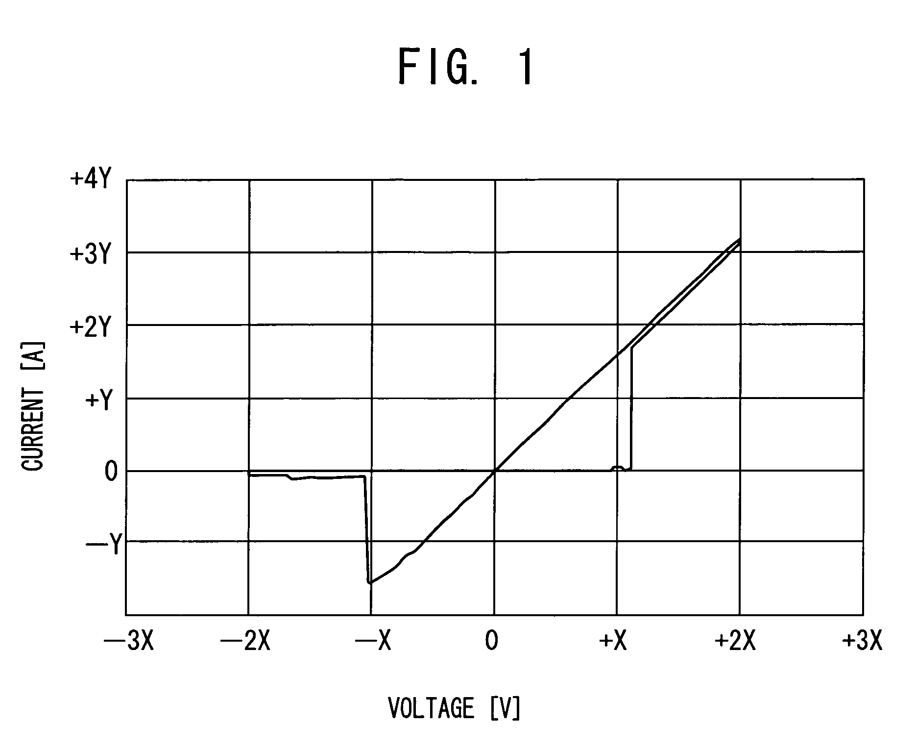
[0093]FIG. 8 shows a relationship between the resistance value immediately after writing into the memory element and the potential applied to the common line in a case where a gate potential (potential applied to the word line) of 2.5 V is applied and the potential between the bit line and the source line of 0.5 V is applied in the memory cell in the above-described circuit diagram shown in FIG. 3.

[0094]FIG. 8 indicates that if the potential applied to the common line is 1.4 V or higher, writing is disabled. This is because as the potential applied to the common line is increased, the gate potential of the MOS transistor relatively becomes lower, that is, the on-resistance of the MOS transistor becomes higher, and the resistance value of the memory element immediately after writing become higher, and thus when the potential applied to the common line is 1.4 V or higher, the potential between the bit line and the common line becomes lower than (voltage threshold of MOS transistor)+(w...


PUM


Abstract

A storage apparatus includes memory devices each having a storage element with a characteristic that the application of an electric signal not lower than a first threshold signal allows the storage element to shift from a high resistance value state to a low resistance value state, and that the application of an electric signal not lower than a second threshold signal, which has a polarity different from that of the first threshold signal, allows the storage element to shift form a low resistance value state to a high resistance value state, and a circuit element connected to the storage element in series to be a load; wherein the memory devices are arranged in a matrix and one terminal of each of the memory devices is connected to a common line; and wherein an intermediate potential between a power supply potential and a ground potential is applied to the common line.

Description

BACKGROUND OF THE INVENTION[0001]1. Field of the Invention[0002]The present invention relates to a storage apparatus and a semiconductor apparatus. More specifically, the present invention relates to a storage apparatus and a semiconductor apparatus which are composed of memory devices each using a storage element storing and holding information according to an electric resistance state.[0003]2. Description of Related Art[0004]In information equipment such as a computer, high density DRAM (Dynamic Random Access Memory) with high operation speed is widely used as a random access memory.[0005]However, since DRAM is volatile memory, which loses information upon turning off power, nonvolatile memory, which holds information after turning off power, has been desired.[0006]As nonvolatile memory which is considered to be promising, there are proposed FeRAM (Ferroelectric Random Access Memory), MRAM (Magnetoresistive Random Access Memory), phase change memory, and resistance change type mem...

Claims


Application Information

Patent Timeline
Patent Type & Authority Patents(United States)
IPC IPC(8): G11C11/00
CPCG11C13/0069G11C13/02G11C2213/79G11C5/063G11C13/0002
Inventor HACHINO, HIDENARIOKAZAKI, NOBUMICHIOTSUKA, WATARUTSUSHIMA, TOMOHITOSAGARA, TSUTOMUNAKASHIMA, CHIEKOMORI, HIRONOBUNAGAO, HAJIME
Owner SONY SEMICON SOLUTIONS CORP
Why Eureka
Try Eureka