Method of manufacturing semiconductor device and apparatus of automatically adjusting semiconductor pattern

a semiconductor and automatic adjustment technology, applied in semiconductor/solid-state device testing/measurement, printing, instruments, etc., can solve the problems of higher process cost than the step & repeat method, not necessarily working well for the exposure process of a pattern, and lower degree of freedom, so as to prevent the occurrence of defective items and improve manufacturing yields. , the effect of reducing the degree of freedom

Inactive Publication Date: 2007-07-17
SONY CORP
View PDF29 Cites 0 Cited by
  • Summary
  • Abstract
  • Description
  • Claims
  • Application Information

AI Technical Summary

Benefits of technology

[0020]As described above, according to the method of manufacturing a semiconductor device in an embodiment of the present invention or the apparatus of automatically adjusting the semiconductor exposure pattern in an embodiment of the present invention, a difference in the shape or position is measured between the first pattern obtained with the exposure method in the first patterning step and the second pattern obtained with the exposure method in the second patterning step having a lower degree of freedom in a manufacturing step cycle of a semiconductor device, and the information on the difference is relied on to adjust the first pattern in a first patterning step with a high degree of freedom such that the shape or position of the first pattern matches the second pattern in a second patterning step with a lower degree of freedom in the next manufacturing step cycle or later of the semiconductor device. Thus, the shape or position of the first pattern in the first patterning step with a high degree of freedom can advantageously match (be aligned with) the second pattern precisely in the second patterning step with a low degree of freedom in the next manufacturing step cycle or later.
[0021]In addition, according to the method of manufacturing a semiconductor device in an embodiment of the present invention, a difference in the shape or position is measured between the first pattern and the second pattern in a lot in the prototyping stage and the measurement results are relied on to adjust the shape of the first pattern in the first patterning step for a production lot. Thus, even if an offset in the shape or position enough to be recognized as a defective item occurs in a lot at the prototyping stage, the first pattern can be precisely aligned with the second pattern in a production lot based on the information on the difference, thereby making it possible to advantageously prevent the occurrence of a defective item to improve manufacturing yields. Furthermore, since the first pattern can be aligned with the second pattern without forming a reference pattern for alignment or the like prior to the first patterning step in a manufacturing process of each wafer or semiconductor device in a production lot, it is possible to avoid a complicated manufacturing method due to an additional step of forming such a reference pattern.

Problems solved by technology

While this exposure step has an advantage of high throughput, it does not necessarily function well for the exposure process of a pattern with a line width design rule of less than 0.25 μm because of limits of resolution or difficulty in making fine adjustments of the pattern during the exposure process.
In this exposure step, however, both stages of a reticule and a wafer must be controlled simultaneously and thus equipment therefore becomes complicated to cause a higher process cost than the step & repeat method.
The exposure step in the step & repeat method, however, allows only scale-up / scale-down and parallel shifts over the entire exposure area with regard to adjustments of the shape or a position of a pattern, so that it has a lower degree of freedom than the exposure step in the scan method.
Thus, if an offset occurs in the shape or the position of the pattern in the exposure step of the scan method performed earlier, a problem arises in that the existing offset cannot be corrected precisely in some cases in the exposure step of the step & repeat method performed later.
For example, if the exposure step in the scan method results in distortion in an aspect ratio over the entire exposure area, the exposure step with the step & repeat method performed thereafter cannot adjust the dimensions independently in the vertical and horizontal directions over the entire exposure area.
For this reason, if adjustments are made to correct the offset only in one of the directions, the offset in the other direction may remain uncorrected or the amount of the offset may increase.
The necessity causes an additional disadvantage of more complicated manufacturing steps or a lower throughput.

Method used


Image

  • Method of manufacturing semiconductor device and apparatus of automatically adjusting semiconductor pattern
  • Method of manufacturing semiconductor device and apparatus of automatically adjusting semiconductor pattern
  • Method of manufacturing semiconductor device and apparatus of automatically adjusting semiconductor pattern

Examples


Embodiment Construction

[0033]A preferred embodiment of the present invention will hereinafter be described in detail with reference to the drawings.

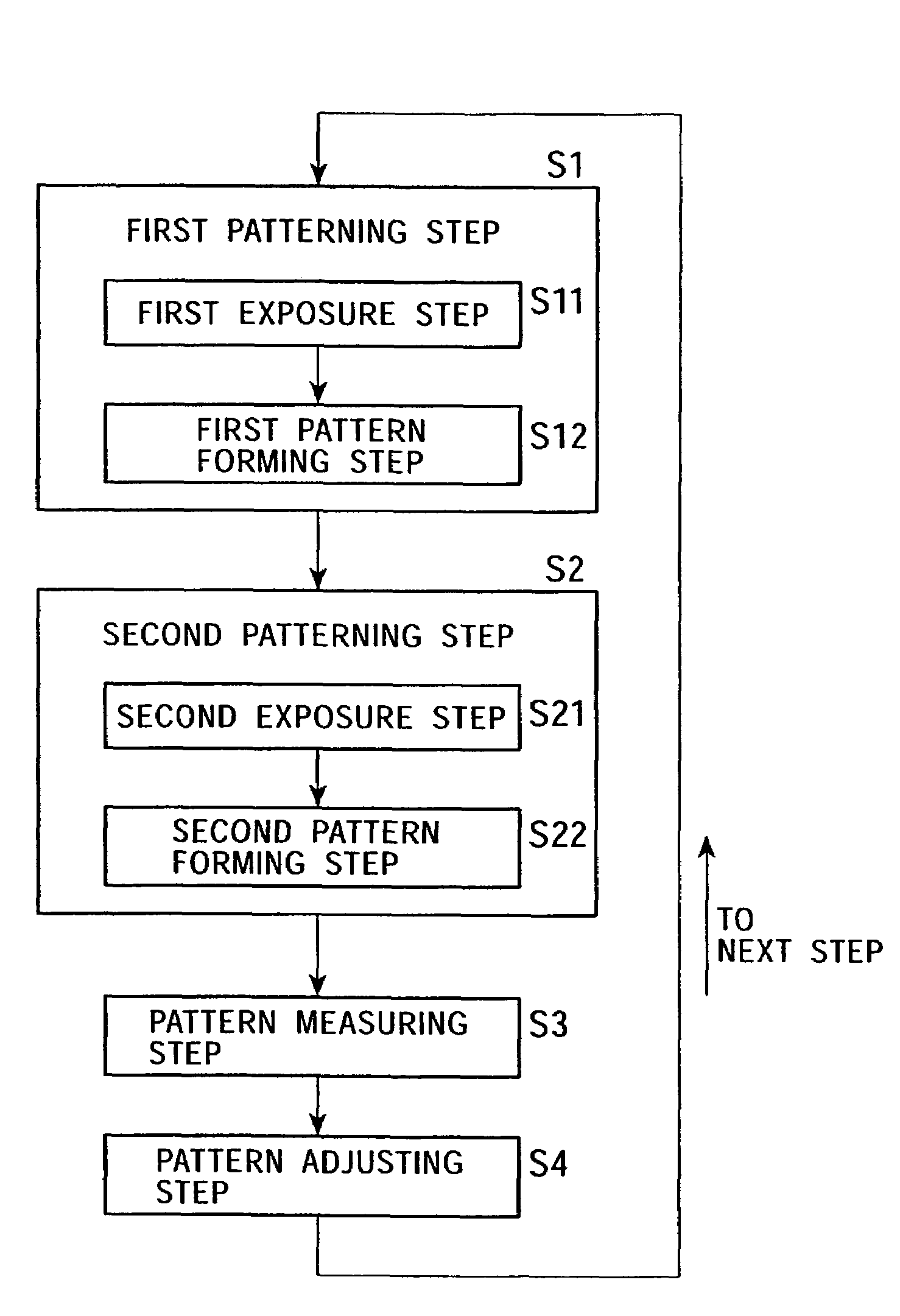
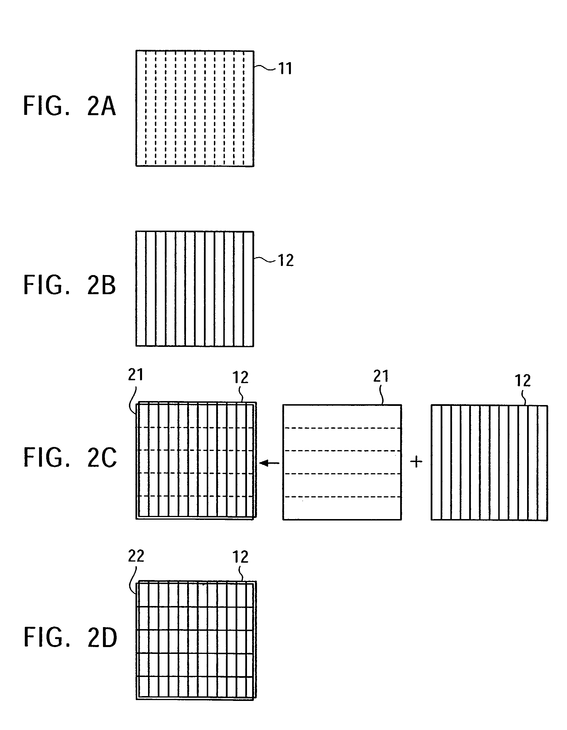
[0034]FIG. 1 illustrates a general flowchart of a method of manufacturing a semiconductor device according to an embodiment of the present invention, and FIGS. 2A to 2D schematically illustrate each step thereof. It should be noted that since a first patterning step, a second patterning step, a pattern measuring step, and a pattern adjusting step are the most important steps in the embodiment and other steps such as a resist applying step or an ion implantation step are conventional ones, the pattern measuring step and the pattern adjusting step as mentioned above are explained in detail especially in the following description to avoid complicated illustration and explanation.

[0035]The method of manufacturing a semiconductor device comprises a first patterning step (S1), a second patterning step (S2), a pattern measuring step (S3), and a pattern adjusting step...


PUM

PropertyMeasurementUnit
widthaaaaaaaaaa
aspect ratioaaaaaaaaaa
shot aspect ratioaaaaaaaaaa

Abstract

A method of manufacturing a semiconductor device and an apparatus of automatically adjusting a semiconductor pattern can precisely correct a difference in the shape or position of a pattern exposed or formed in two exposure steps. A pattern measuring unit measures an offset between the first pattern and the second pattern in a pattern measuring step. Based on the information on the offset thus detected, the first pattern is adjusted in a first patterning step with a high degree of freedom in the next manufacturing step cycle of a semiconductor device to precisely align the shape or position of the first pattern with the second pattern in a second patterning step with a low degree of freedom.

Description

RELATED APPLICATION DATA[0001]The present application claims priority to Japanese Application No. P2000-325173, filed Oct. 25, 2000, and is a divisional of U.S. application Ser. No. 10 / 037,988, filed Oct. 23, 2001, now U.S. Pat. No. 6,537,835 both of which are incorporated herein by reference to the extent permitted by law.CROSS REFERENCES TO RELATED APPLICATIONS[0002]The present invention claims priority to priority document no. 2000-325173 filed in Japan on Oct. 25, 2000, and incorporated by reference herein.BACKGROUND OF THE INVENTION[0003]1. Field of the Invention[0004]The present invention relates to a method of manufacturing a semiconductor device including a step of exposing a fine pattern with precise alignment, and an apparatus of automatically adjusting a semiconductor exposure pattern for use in the method.[0005]2. Description of Related Art[0006]In semiconductor devices such as so-called integrated circuits, a finer pattern and a higher integration degree are recently re...

Claims


Application Information

Patent Timeline
Patent Type & Authority Patents(United States)
IPC IPC(8): H01L21/66G01B11/00G01B11/14G01R31/26G03B27/42G03F7/20G03F7/22G03F9/00H01L21/027
CPCG03F7/7045G03F7/70458G03F9/7003H01L22/20Y10S438/947H01L2924/0002Y10S438/942H01L2924/00
Inventor ADACHI, NAOYASUSUZUKI, KATSUYANOGUCHI, MASAYUKI
Owner SONY CORP
Why Eureka
Try Eureka