
Exposed lead interposer leadframe package

Active Publication Date: 2007-07-17
AMKOR TECH SINGAPORE HLDG PTE LTD
View PDF355 Cites 119 Cited by
  • Summary
  • Abstract
  • Description
  • Claims
  • Application Information

AI Technical Summary

Benefits of technology

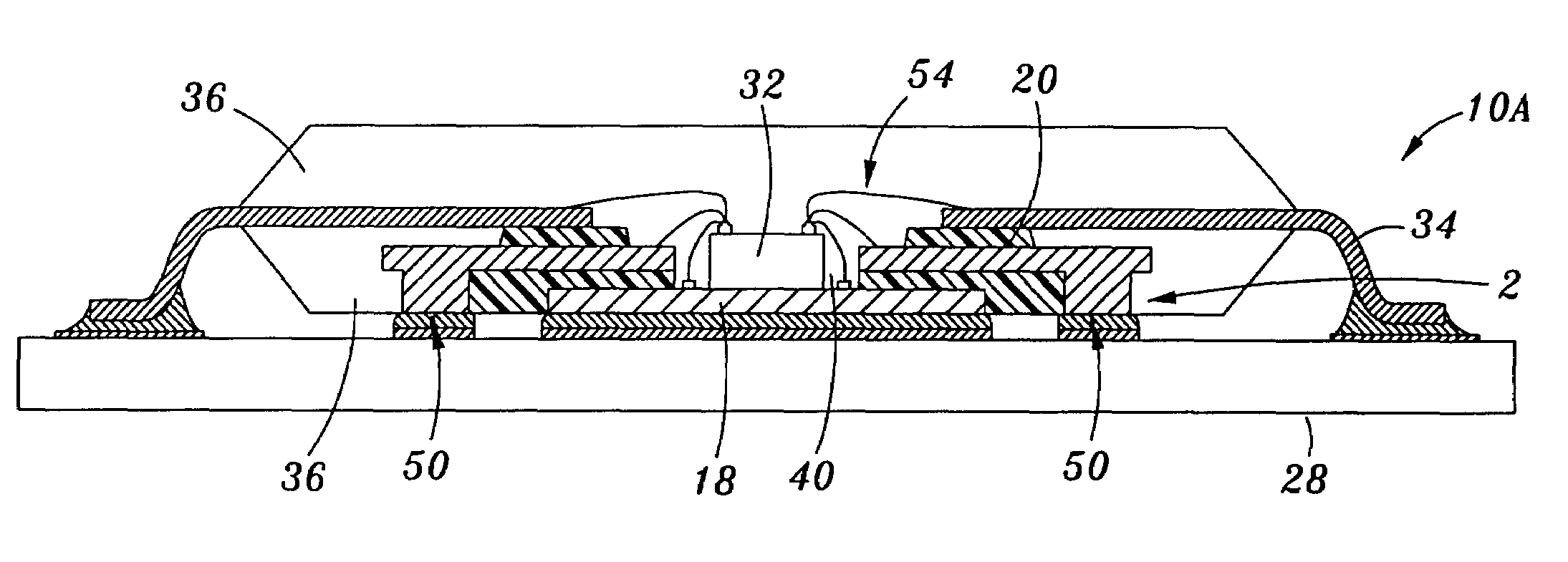
[0009]The aforementioned disadvantages are overcome by providing a separate interposer structure which may be integrated into a semiconductor package. Furthermore, the present invention provides a semiconductor package which integrates a separate interposer with an external lead semiconductor package or land pattern semiconductor package to increase the total input / output capabilities of the semiconductor package.
[0010]The interposer constructed in accordance with the present invention is adapted to be integrated into either external lead semiconductor packages such as a quad flat package (QFP), thin quad flat package (TQFP), or thin small outline package (TSOP). In addition to external lead packages, the interposer of the present invention may be integrated into a land pattern semiconductor package such as a micro lead frame package. When integrated into either an external lead semiconductor package or a land pattern semiconductor package, the interposer provides such package with independent exposed lands which supplement the external leads normally provided with an external lead semiconductor package and the exposed pads normally provided with a land pattern semiconductor package. The added lands provide greater design flexibility, and the capability of standardizing the package footprint without constraints on the size of the semiconductor die of the package.
[0011]The interposer of the present invention also provides the advantages of allowing standard external lead semiconductor packages and land patterns semiconductor packages to be retrofitted with the interposer to allow for the use in the package of a die having an increased number of I / O's. The ability to accommodate the increased I / O semiconductor die is facilitated by the additional lands defined by the interposer. The interposer of the present invention also cost effectively adds additional I / O paths to semiconductor packages, and creates high frequency electrical signal I / O paths on the bottom of the package body of the semiconductor package without degrading the electrical performance thereof. Furthermore, the interposer of the present invention will allow QFP's to have operational frequencies beyond five GHz in a cost effective matter. The interposer of the present invention also provides a cost effective alternative to exposed lead semiconductor packages wherein additional I / O paths are provided as a result of the implementation of a partial saw process. In this regard, by utilizing the interposer, such partial saw process may be eliminated since the interposer may be fabricated separately from the lead frame of the external lead or land pattern semiconductor package.

Problems solved by technology

Current designs of standard external lead packages, such as a quad flat package (QFP), thin quad flat package (TQFP) or thin small outline package (TSOP) are not well suited or easily adaptable for the increased number of I / O leads that current state of the art dies require.
Furthermore, external lead packages are still utilized in many electronic devices and many manufacturers do not desire to completely redesign their current motherboard layouts to accommodate semiconductor packages having increased I / O specifications.
Moreover, die I / O requirements are even out pacing many of the current land pattern package I / O capabilities, such as micro leadframe packages currently utilized my many electronic manufacturers.

Method used


Image

  • Exposed lead interposer leadframe package
  • Exposed lead interposer leadframe package
  • Exposed lead interposer leadframe package

Examples


third embodiment

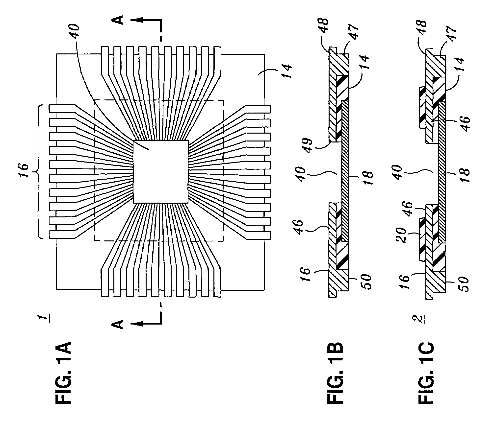
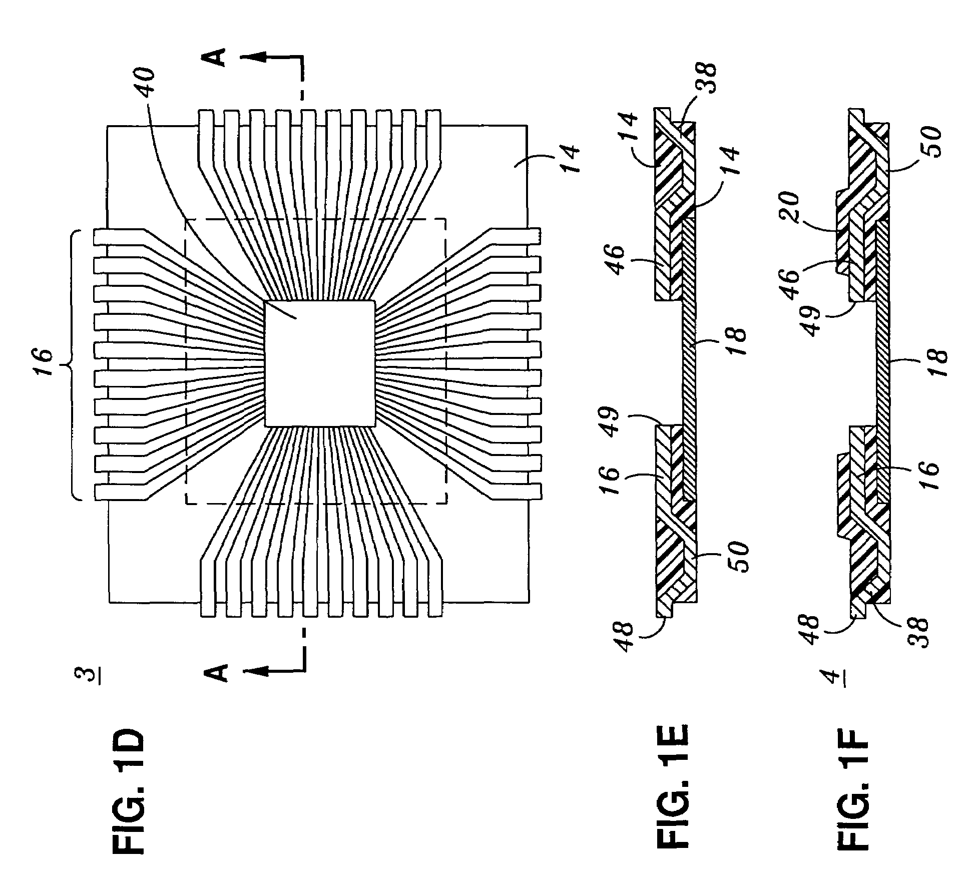
[0059]The interposer 3 has features similar to those of the interposers 1, 2 above, except for the specific design of the interposer leads 16 used in interposer 3. In the third embodiment, interposer leads 16 each have a downset 38 which defines a land 50 (or exposed lead). In the “downset molded” interposer 3, the lands 50 are positioned closer toward the peripheral edge of die pad 18, as compared to the lands 50 in the interposers 1, 2. In particular, the downset 38 begins at about a thirty to forth-five degree angle downward just above the peripheral edge of die pad 18, and then straightens out so that the land 50 is generally co-planar with the bottom surface of the die pad 18. The downset 38 then returns upward at about a thirty to forty-five degree angle until it reaches the exterior terminal end 48 of the corresponding interposer lead 16. Land 50 provides an exposed lead or pad on the lower surface of the interposer 3 which may be utilized as a solder connection terminal for ...

fifth embodiment

[0062]In the fifth embodiment, die pad 18 and the interposer leads 16 are the same as those described in the previous embodiments; however, the “½ etch with tape” interposer 5 does not include the molded dielectric 14. Instead, interposer 5 utilizes a nonconductive adhesive tape 22 or similar material that acts as a structural member to connect the undersides of finger portions 46 of the interposer leads 16 to a peripheral portion of the top surface of die pad 18. This embodiment is ideally suited for less complex exposed lead structures that are less prone to damage or stability problems.

[0063]In particular, adhesive tape 22 is applied to the top surface of die pad 18 along the square or rectangular outer peripheral edge of die pad 18. A portion of die pad 18 is left uncovered to receive die 32. The interposer leads 16 are shaped and arranged in a similar manner as those described in the first embodiment (see “½ etch molded interposer 1”). However, in the interposer 5 the lower sur...

eighth embodiment

[0071]FIG. 3B is a cross-sectional view of an eighth exemplary embodiment of the present invention in which an exposed lead semiconductor package 10B is provided with the “½ etch molded” interposer 1 shown and described in relation to FIGS. 1A and 1B. In the semiconductor package 10B, adhesive tape 23 is substituted for the pedestal 20 of the interposer 2. In this regard, the fabrication process associated with the semiconductor package 10B of the eighth embodiment is substantially identical to that described above in relation to the semiconductor package 10A, except that the inner portions of the leads 34 of the leadframe in the semiconductor package 10B are adhered to the adhesive tape 23, as opposed to being interfaced to the pedestal 20 of the interposer 2 as described in relation to FIG. 10A. In fabricating the semiconductor package 10B, the adhesive tape 23 should be sufficiently thick to ensure a low coupling capacitance between the leads 34 of the leadframe and the interpose...


PUM


Abstract

An interposer for use in an external lead or land pattern semiconductor package. The interposer includes an interposer body which is molded from a dielectric material. The interposer body defines opposed top and bottom surfaces, an outer peripheral edge, and an inner peripheral edge. Embedded within the interposer body is a die pad which itself defines opposed top and bottom surfaces and a peripheral edge. The bottom surface of the die pad is exposed in and substantially flush with the bottom surface of the interposer body, with the inner peripheral edge of the interposer body and the top surface of the die pad collectively defining a cavity of the interposer. A plurality of electrically conductive interposer leads are embedded within the top surface of the interposer body and at least partially exposed therein. The interposer body forms a nonconductive barrier between each of the interposer leads and between the interposer leads and the die pad.

Description

CROSS-REFERENCE TO RELATED APPLICATIONS[0001](Not Applicable)STATEMENT RE: FEDERALLY SPONSORED RESEARCH / DEVELOPMENT[0002](Not Applicable)BACKGROUND OF THE INVENTION[0003]1. Field of the Invention[0004]The present invention relates to the field of semiconductor packaging. In particular, the present invention relates to a separate interposer structure which may be utilized in a semiconductor package to increase the total input / output capabilities of the semiconductor package.[0005]2. Background Information[0006]As a result of continuing improvements in semiconductor technology, the specified number of input / output (I / O) leads required to be connected to silicon dies continues to increase. Current designs of standard external lead packages, such as a quad flat package (QFP), thin quad flat package (TQFP) or thin small outline package (TSOP) are not well suited or easily adaptable for the increased number of I / O leads that current state of the art dies require. Furthermore, external lea...

Claims


Application Information

Patent Timeline
IPC IPC(8): H01L23/02
CPCH01L23/49527H01L23/49531H01L23/49551H01L23/49861H01L24/49H01L25/105H01L24/45H01L2224/45144H01L2224/48091H01L2224/48247H01L2224/49109H01L2224/73265H01L2924/01005H01L2924/01014H01L2924/01027H01L2924/01029H01L2924/01075H01L2924/01079H01L2924/01082H01L2924/15153H01L2924/1517H01L2924/1532H01L2924/3011H01L2924/00014H01L2924/00H01L24/48H01L2224/32245H01L2924/01033H01L2924/014H01L2225/1029H01L2225/1041H01L2924/10253H01L2924/181H01L2224/85207H01L2924/00012
Inventor FOSTER, DONALD CRAIG
Owner AMKOR TECH SINGAPORE HLDG PTE LTD
Learn More