Nonvolatile semiconductor memory

a non-volatile, semiconductor technology, applied in semiconductor devices, digital storage, instruments, etc., can solve problems such as increasing the surface area of semiconductor chips

Active Publication Date: 2007-07-17
KIOXIA CORP
View PDF15 Cites 61 Cited by
  • Summary
  • Abstract
  • Description
  • Claims
  • Application Information

AI Technical Summary

Problems solved by technology

However, in order to increase the value of the breakdown voltage, things like the gate length and the distance between the gate electrode and the contact must be set wider, which presents the problem of increased surface area of the semiconductor chip (see, for instance, Japanese Patent Application Laid-open No. 2002-141477, in particular, FIG. 7.).

Method used


Image

  • Nonvolatile semiconductor memory
  • Nonvolatile semiconductor memory
  • Nonvolatile semiconductor memory

Examples


first embodiment

[First Embodiment]

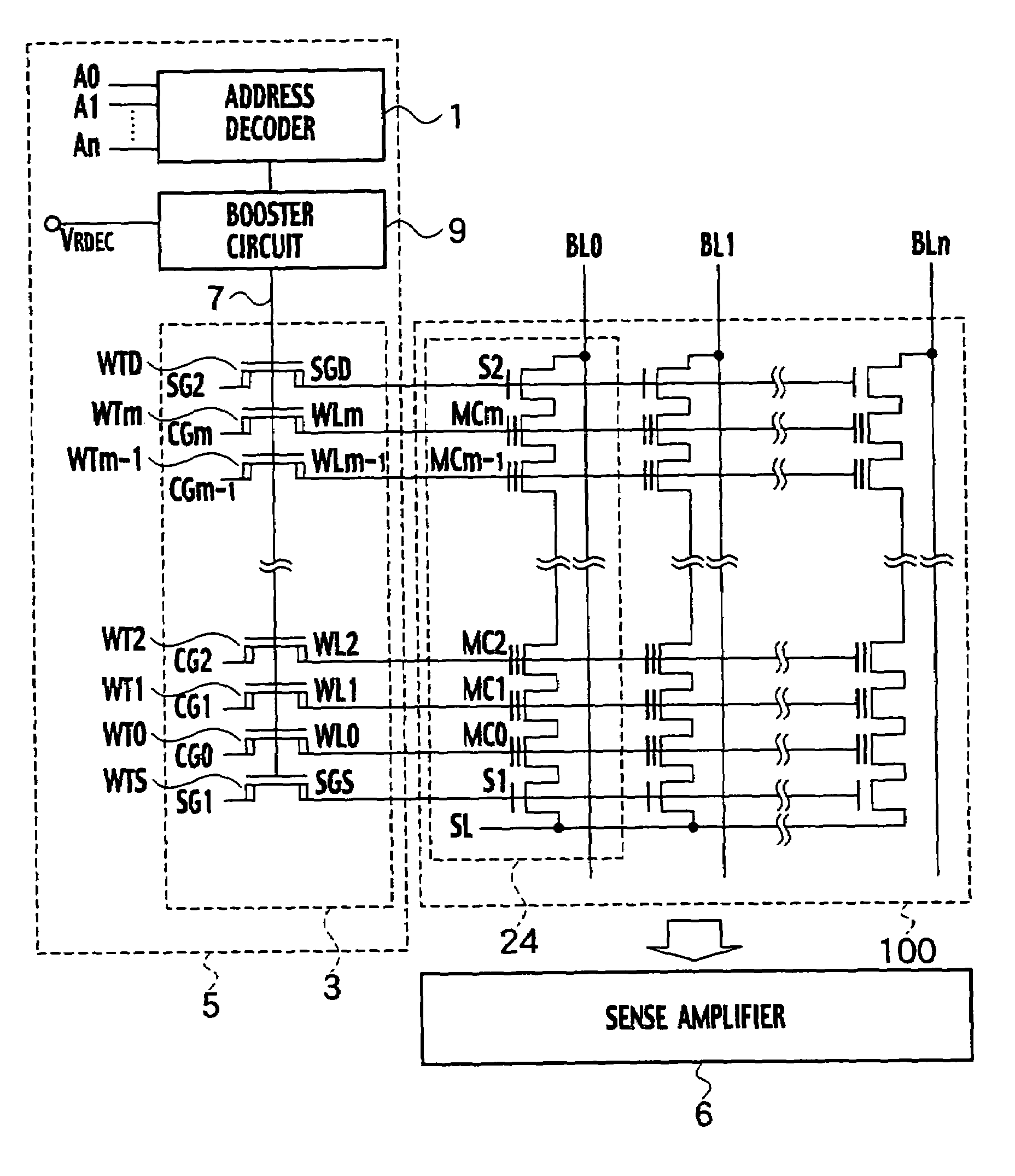
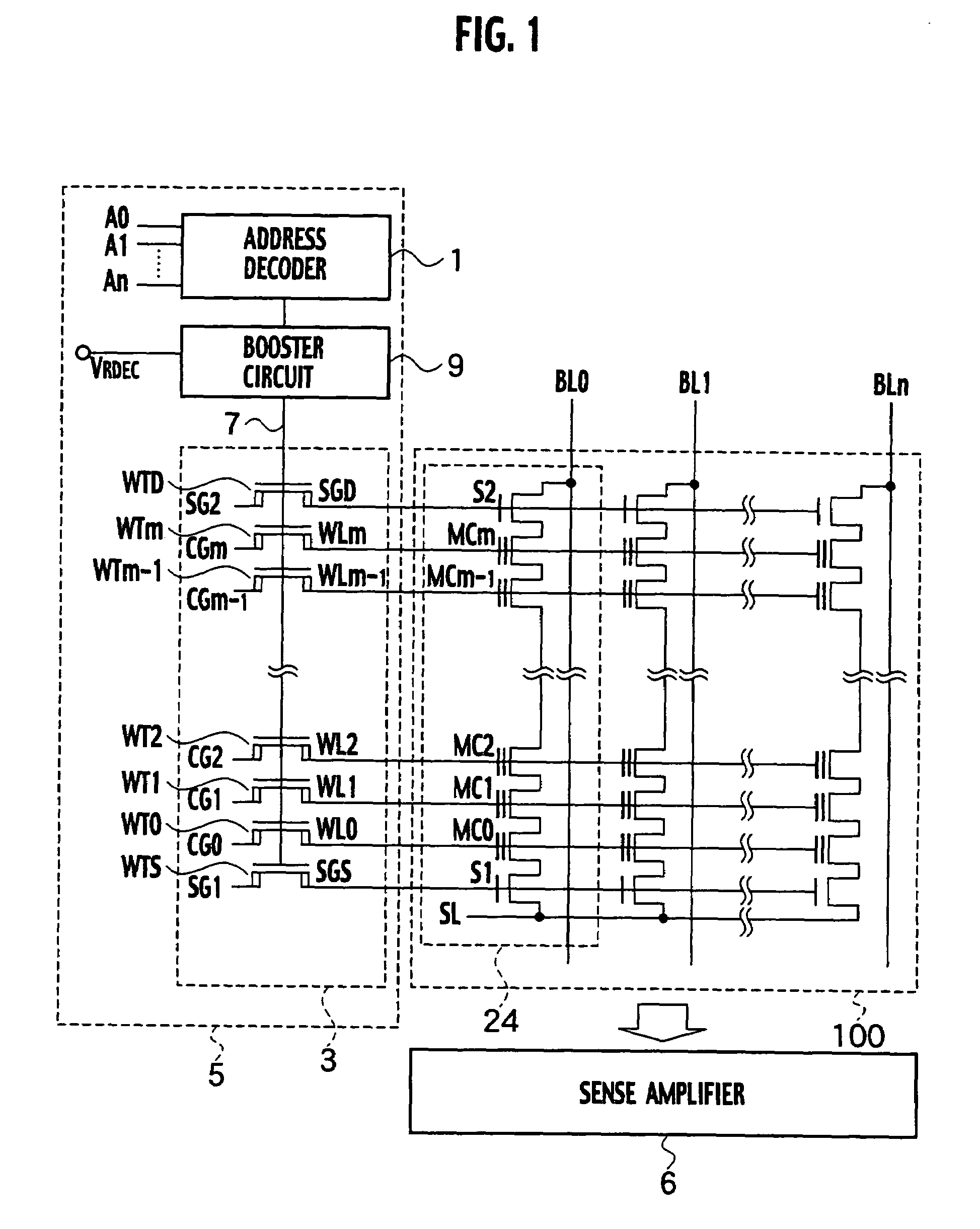
[0095]The nonvolatile semiconductor memory device according to the first embodiment of the present invention, as shown in FIG. 1, is constituted by a memory cell array 100, a row decoder 5, and a sense amplifier 6, in an instance where the memory cell array is composed of a NAND type EEPROM. The memory cell array 100 includes memory cell transistors MC that are disposed at the intersections of the plurality of word lines WL0 through WLm that span in rows, and the plurality of bit lines that span in columns. The row decoder 5 is disposed on the periphery of the memory cell array 100. The row decoder 5 includes a word line transfer transistor unit 3, a booster circuit 9, and an address decoder 1. The memory cell array 100 further includes a NAND cell unit 24. The NAND cell unit 24 is constituted by a plurality of memory cell transistors MC0 through MCm that are connected in series in between select gate transistors S2 on a bit line BL side and select gate transistors...

second embodiment

[Second Embodiment]

(Fourth Example of a Layout Pattern of the Word Line Transfer Transistors)

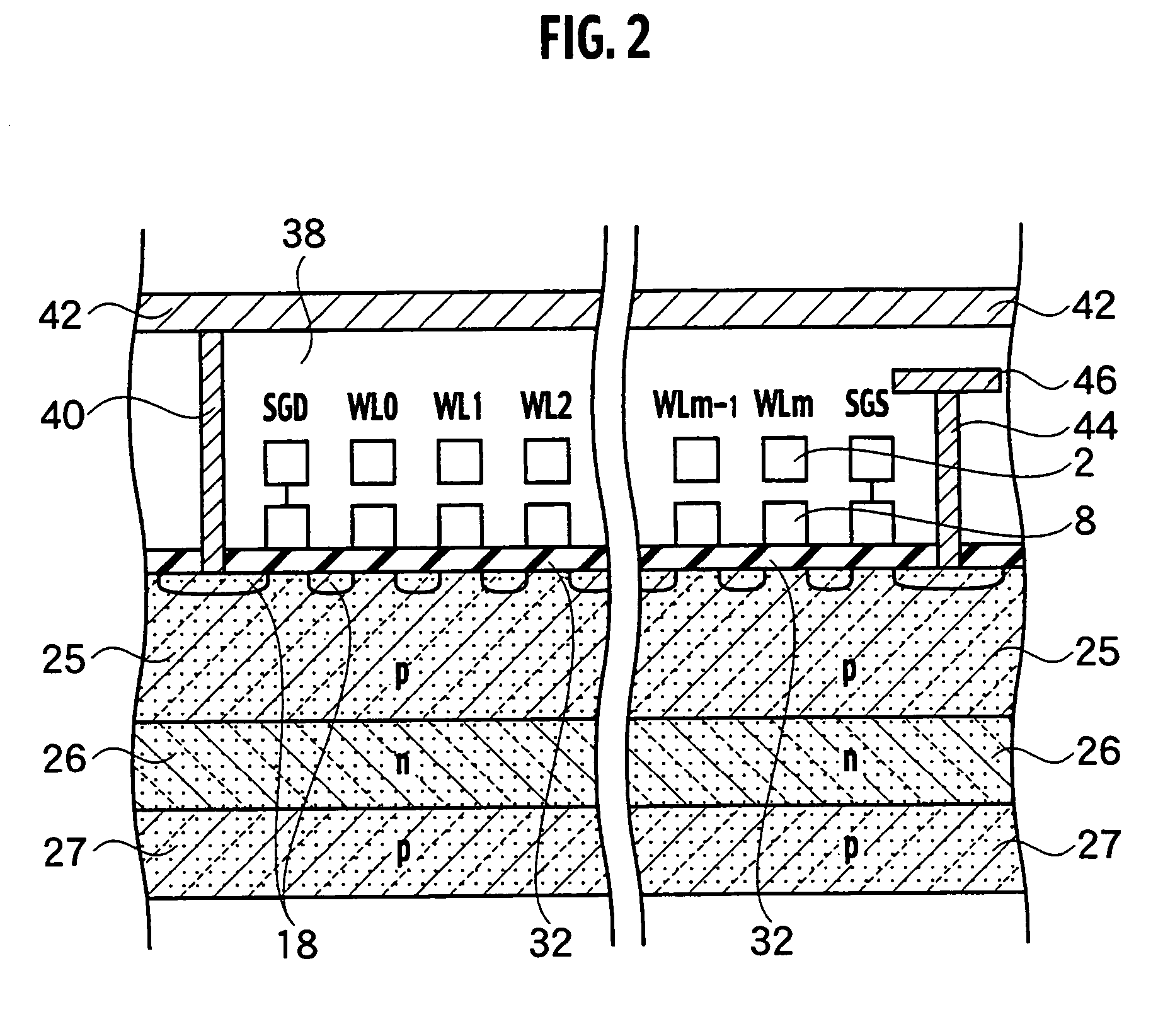
[0144]The constitution of another layout pattern of the four adjacent word line transfer transistors of the nonvolatile semiconductor memory device according to the first embodiment of the present invention includes the active areas 16-1, 16-2, and 17-1, 17-2 of the word line transfer transistors aligned in two rows, the word line contact plug 48 and CG line contact plug 49 formed inside of the active areas 16-1, 16-2, and 17-1, 17-2, the gate electrodes 15a and 15b, the element isolation region 28, and the field stopper p+ layer 34, as shown in FIG. 30. The gate electrodes 15a and 15b are connected in common with the gates of the word line transfer transistors aligned in rows, and the element isolation region 28 separates each of the active areas 16-1, 16-2, and 17-1, 17-2 from each other, and the field stopper p+ layer 34 is disposed on the bottom of the element isolation region 28.

[0145]I...

third embodiment

[Third Embodiment]

[0164]The nonvolatile semiconductor memory device according to the third embodiment of the present invention is constituted by, as shown in FIG. 35, the memory cell array 100, a switching transistor unit 90, the sense amplifier 6, and a shield power supply 110, in the case the memory cell array is constituted by a NAND type EEPROM. The memory cell array 100 includes memory cell transistors MC disposed at the intersection of the plurality of word lines WL0 through WLm spanning in rows and the plurality of bit lines BL0 through BLn spanning in columns. The two bit-line switching transistor units 90 are disposed in the periphery of the memory cell array 100.

[0165]Concerning the row decoder 5 shown on the nonvolatile semiconductor memory device according to the first embodiment of the present invention, illustration has been omitted from FIG. 35. Here, in the same fashion as in FIG. 1, it is acceptable to establish the word line transfer transistor unit 3 and elaborate...


PUM


Abstract

A nonvolatile semiconductor memory includes: a memory cell array constituted by word lines, bit lines, and electrically erasable / rewritable memory cell transistors, which have respective tunnel insulating films and are arranged at the intersections of the word lines and the bit lines; and a word line transfer transistor, which is separated by an element isolation region, has a source diffusion layer, a channel region, a gate insulating film on the channel region, and a drain diffusion layer, and is connected to a word line and a gate electrode formed on the gate insulating film via a word line contact plug formed in the drain diffusion layer. The channel width of the word line transfer transistor is at least six times width of the word line contact plug, and the distance in a second direction between the word line contact plug and corresponding element isolation region is greater than distance in a first direction between the word line contact plug and corresponding element isolation region where, the first direction denotes a direction from the source diffusion layer towards the drain diffusion layer, and the second direction denotes a direction perpendicular to the first direction.

Description

CROSS REFERENCE TO RELATED APPLICATIONS AND INCORPORATION BY REFERENCE[0001]This application is based upon and claims the benefit of priority from prior Japanese Patent Application P2004-162276 filed on May 31, 2004; the entire contents of which are incorporated by reference herein.BACKGROUND OF THE INVENTION[0002]1. Field of the Invention[0003]The present invention relates to an electrically rewriteable / erasable semiconductor memory device, and more particularly to a non-volatile semiconductor memory having peripheral circuits constituted by high voltage transistors.[0004]2. Description of the Related Art[0005]In a NAND type EEPROM, a type of nonvolatile semiconductor memory device, a high voltage programming write-in voltage Vpgm is applied to the word line during NAND cell programming. The programming write-in voltage Vpmg is supplied by the word line drive signal lines CG0 to CGm (m is a natural number). A word line transmission transistor is disposed in between the word line dr...

Claims


Application Information

Patent Timeline
Patent Type & Authority Patents(United States)
IPC IPC(8): G11C11/34H01L27/10G11C8/00G11C8/10G11C16/04G11C16/08G11C16/10H01L21/8247H01L27/115H01L29/788H01L29/792
CPCG11C8/10G11C16/0483G11C16/08G11C16/10H01L27/115H01L27/11521H10B69/00H10B41/30H10B41/35
Inventor GODA, AKIRANOGUCHI, MITSUHIROKAJIMOTO, MINORITAKEUCHI, YUJI
Owner KIOXIA CORP
Why Eureka
Try Eureka