Differential buffer circuit with reduced output common mode variation

a buffer circuit and common mode variation technology, applied in logic circuit coupling/interface arrangement, digital transmission, pulse technique, etc., can solve the problem of reducing the effectiveness of the control reference circuit in controlling the output common mode voltage of the buffer circuit, general insufficient control of the output common mode variation, and overall inaccuracy of the control reference circuit. the effect of reducing the silicon area required by the differential buffer circui

Inactive Publication Date: 2007-07-24
AVAGO TECH WIRELESS IP SINGAPORE PTE
View PDF11 Cites 20 Cited by
  • Summary
  • Abstract
  • Description
  • Claims
  • Application Information

AI Technical Summary

Benefits of technology

[0006]The present invention meets the above-noted need by providing, in an illustrative embodiment, an improved differential buffer circuit capable of exhibiting a reduced output common mode voltage. To accomplish this, the illustrative differential buffer circuit incorporates a common mode control circuit, thereby providing local feedback control without requiring the use of a local operational amplifier and related compensation circuitry. Consequently, the silicon area required by the differential buffer circuit is advantageously reduced compared to conventional differential buffer circuit configurations.

Problems solved by technology

This approach, however, generally does not provide sufficient control of the output common mode variation as may be required to meet a particular standard due, at least in part, to direct current (DC) offsets in operational amplifiers (opamps) used in the control reference circuit and / or buffer circuit, relative voltage (current-resistance (IR)) drops between the PVT control reference circuit and the buffer circuit, and / or device mismatches between the replica bias circuitry and the buffer circuit.
Each of these factors contributes to an overall inaccuracy of the control reference circuit and hence reduces an effectiveness of the control reference circuit in controlling the output common mode voltage of the buffer circuit.
Therefore, the total number of PVT reference circuits required in a given IC undesirably increases, especially in integrated circuits utilizing a large number of buffer circuits.
This substantially increases a cost of the IC.

Method used


Image

  • Differential buffer circuit with reduced output common mode variation
  • Differential buffer circuit with reduced output common mode variation
  • Differential buffer circuit with reduced output common mode variation

Examples


Embodiment Construction

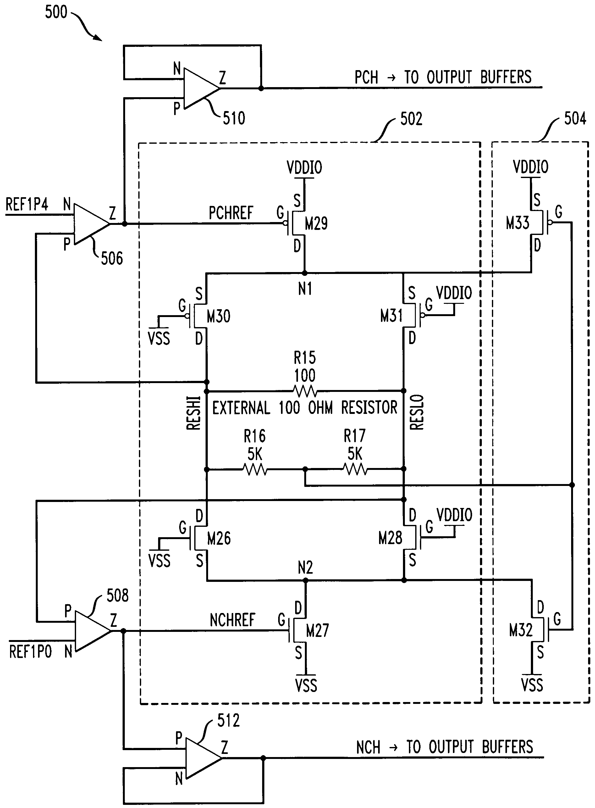
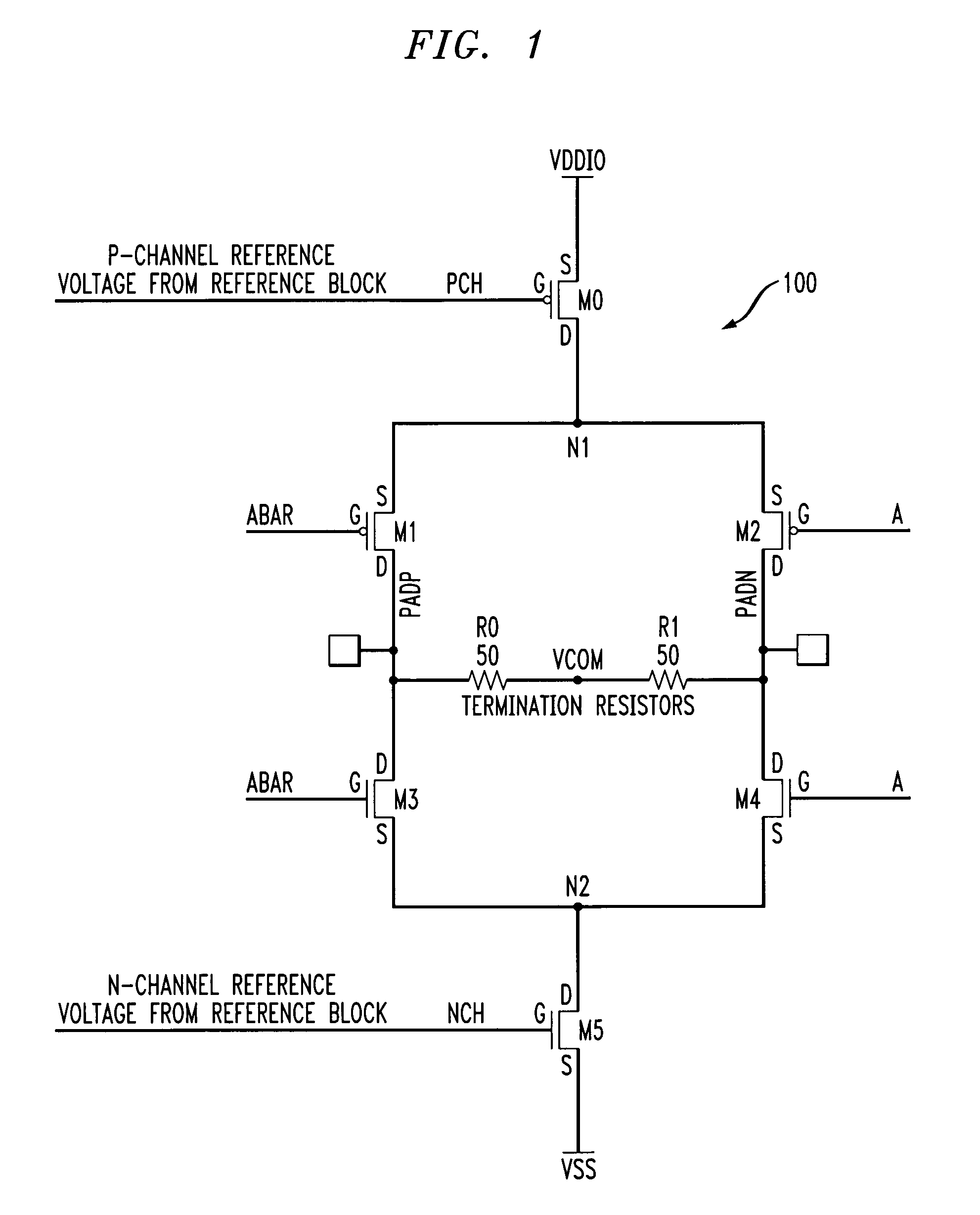
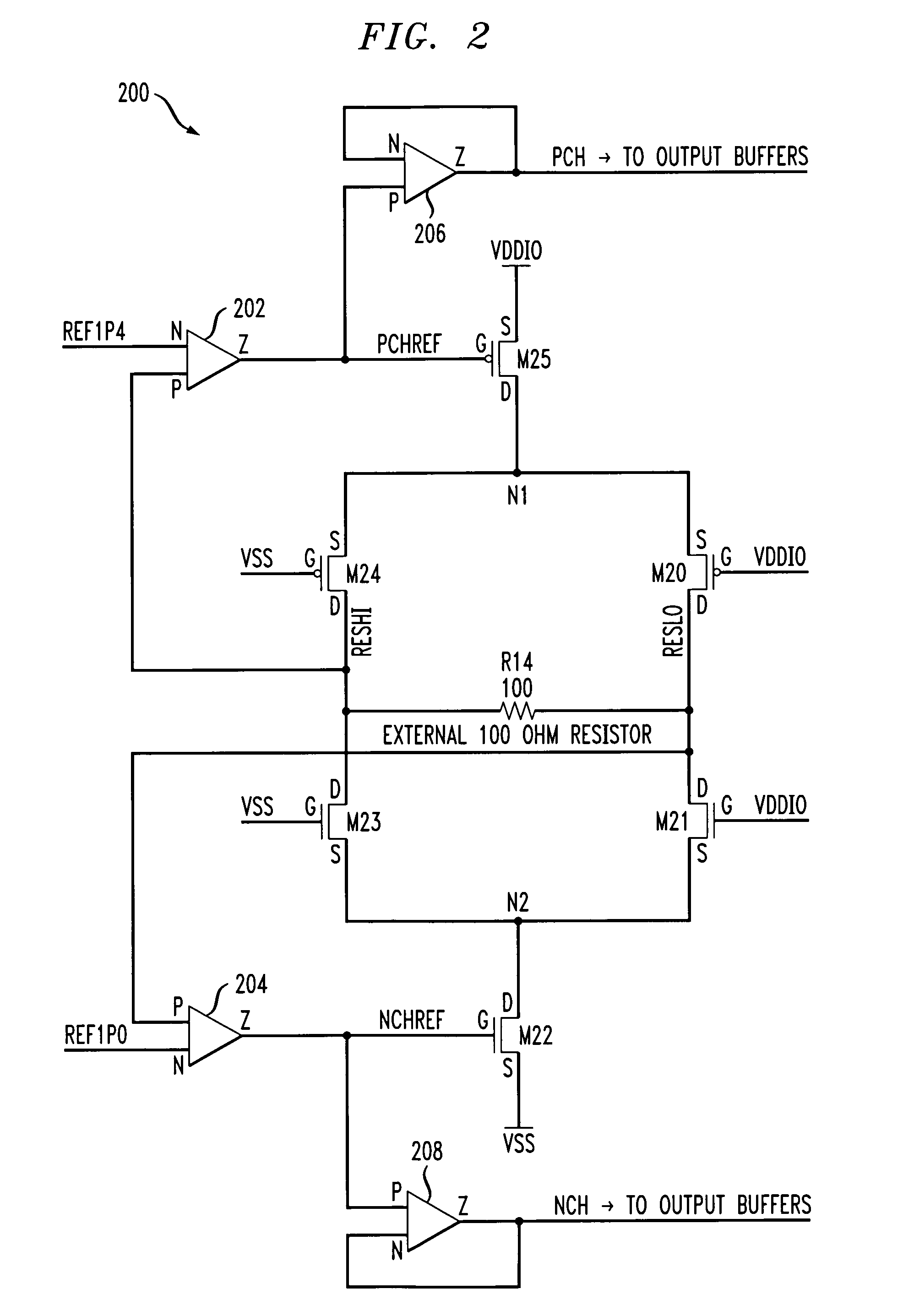
[0017]The present invention will be described herein in the context of illustrative LVDS buffer circuits. It should be understood, however, that the present invention is not limited to these or any other particular circuit arrangements. Rather, the invention is more generally applicable to techniques for reducing output offset voltage, commonly referred to as output common mode voltage, in a differential buffer circuit. Although implementations of the present invention are described herein with specific reference to p-channel metal-oxide-semiconductor (PMOS) and n-channel metal-oxide-semiconductor (NMOS) transistor devices, as may be formed using a complementary metal-oxide-semiconductor (CMOS) fabrication process, it is to be understood that the invention is not limited to such transistor devices and / or such a fabrication process, and that other suitable devices, such as, for example, bipolar junction transistors (BJTs), etc., and / or fabrication processes (e.g., bipolar, BiCMOS, et...


PUM


Abstract

A differential buffer circuit includes a current source, a current sink, and a switching circuit connected to the current source at a first node and connected to the current sink at a second node. The switching circuit is operative to selectively control a direction of current flowing through differential outputs of the buffer circuit in response to at least a first control signal. The buffer circuit further includes a common mode detection circuit and a common mode control circuit. The common mode detection circuit is operative to detect an output common mode voltage of the buffer circuit and to generate a second control signal representative of the output common mode voltage. The common mode control circuit includes a first terminal connected to the current source and a second terminal connected to the current sink. The common mode control circuit is operative to selectively control the output common mode voltage of the buffer circuit as a function of the second control signal.

Description

FIELD OF THE INVENTION[0001]The present invention relates generally to electronic circuits, and more particularly relates to enhanced differential buffer circuits.BACKGROUND OF THE INVENTION[0002]Buffer circuits (e.g., output buffers and bidirectional buffers) are employed in a variety of electronic devices and applications, particularly networking applications involving high-speed data transfer applications. In order to ensure interoperability between such electronic devices, differential input / output (I / O) buffers are often employed which comply with a set of electrical specifications set forth in one or more standards. One common standard for differential I / O interfaces is the Institute of Electrical and Electronics Engineers (IEEE) 1596.3 standard for low-voltage differential signaling (LVDS). The IEEE 1596.3 standard specifies signaling levels for the high-speed / low-power physical layer interface. It also defines the common mode range of an LVDS buffer. The IEEE 1596.3 standard...

Claims


Application Information

Patent Timeline
Patent Type & Authority Patents(United States)
IPC IPC(8): H03K19/0175
CPCH04L25/0276
Inventor BHATTACHARYA, DIPANKARKOTHANDARAMAN, MAKESHWARKRIZ, JOHN C.MORRIS, BERNARD L.
Owner AVAGO TECH WIRELESS IP SINGAPORE PTE
Why Eureka
Try Eureka