Semiconductor device for driving a current load device and a current load device provided therewith

Active Publication Date: 2007-08-14
GOLD CHARM LTD
View PDF12 Cites 78 Cited by
  • Summary
  • Abstract
  • Description
  • Claims
  • Application Information

AI Technical Summary

Benefits of technology

[0021]It is an object of the present invention to provide a semiconductor device for driving a light emission display device and a light emission display device provided therewith capable of s

Problems solved by technology

In case of voltage output, since unevenness of threshold of a transistor and unevenness of voltage-current characteristics and current-brightness characteristics of the luminous element are present in a pixel circuit (1-pixel display portion), even if the same voltage is applied, there is a high possibility that brightness is uneven.
However, in a transistor, particularly in TFT, since unevenness of current abilities where the same gate voltage is applied between different TFTs is great, there poses a problem that it is difficult to issue a current output of high accuracy.
Further, current abilities become uneven even between TFTs as in a close area, an

Method used


Image

  • Semiconductor device for driving a current load device and a current load device provided therewith
  • Semiconductor device for driving a current load device and a current load device provided therewith
  • Semiconductor device for driving a current load device and a current load device provided therewith

Examples


first embodiment

[0128] as described above, it is possible to supply current at high speed and with high accuracy to a light emission display device having a P channel TFT as shown in FIG. 4A.

[0129]Next, the second embodiment of the present invention will be explained. In the second embodiment, the constitution of the 1-bit D / I conversion portion in the first embodiment is changed, and for example, the second embodiment is applied to the pixel circuit shown in FIG. 4B. FIG. 12 is a block diagram showing the constitution of a 1-bit D / I conversion portion according to a second embodiment of the present invention.

[0130]A 1-bit D / I conversion portion 231a according to the second embodiment is provided with a P channel TFT T2 in place of the N channel TFT T1 in the first embodiment, to which source and one end of the capacity element C1 are supplied a power supply potential VD. The voltage VD is a voltage equal to or lower than the voltage VEL, which is a level not posing a problem in terms of operation....

third embodiment

[0134]In a 1-bit D / I conversion portion 231b a suitable stabilized voltage VB instead of the ground potential GND is supplied to one end of the capacity element C1.

[0135]The operation of the third embodiment is similar to the first embodiment, and the similar effect is obtained. This indicates that the voltage supplied to the capacity element C1 may be any voltage as long as it is stabilized. Next, the fourth embodiment of the present invention will be explained. In the fourth embodiment, the constitution of the 1-bit D / I conversion portion in the first embodiment is changed, and for example, the fourth embodiment is applied to the pixel circuit shown in FIG. 4B. FIG. 14 is a block diagram showing the constitution of a 1-bit D / I conversion portion according to the fourth embodiment of the present invention.

[0136]In a 1-bit D / I conversion portion 231c according to the fourth embodiment, a suitable stabilized voltage VB instead of the ground potential GND is supplied to one end of th...

seventh embodiment

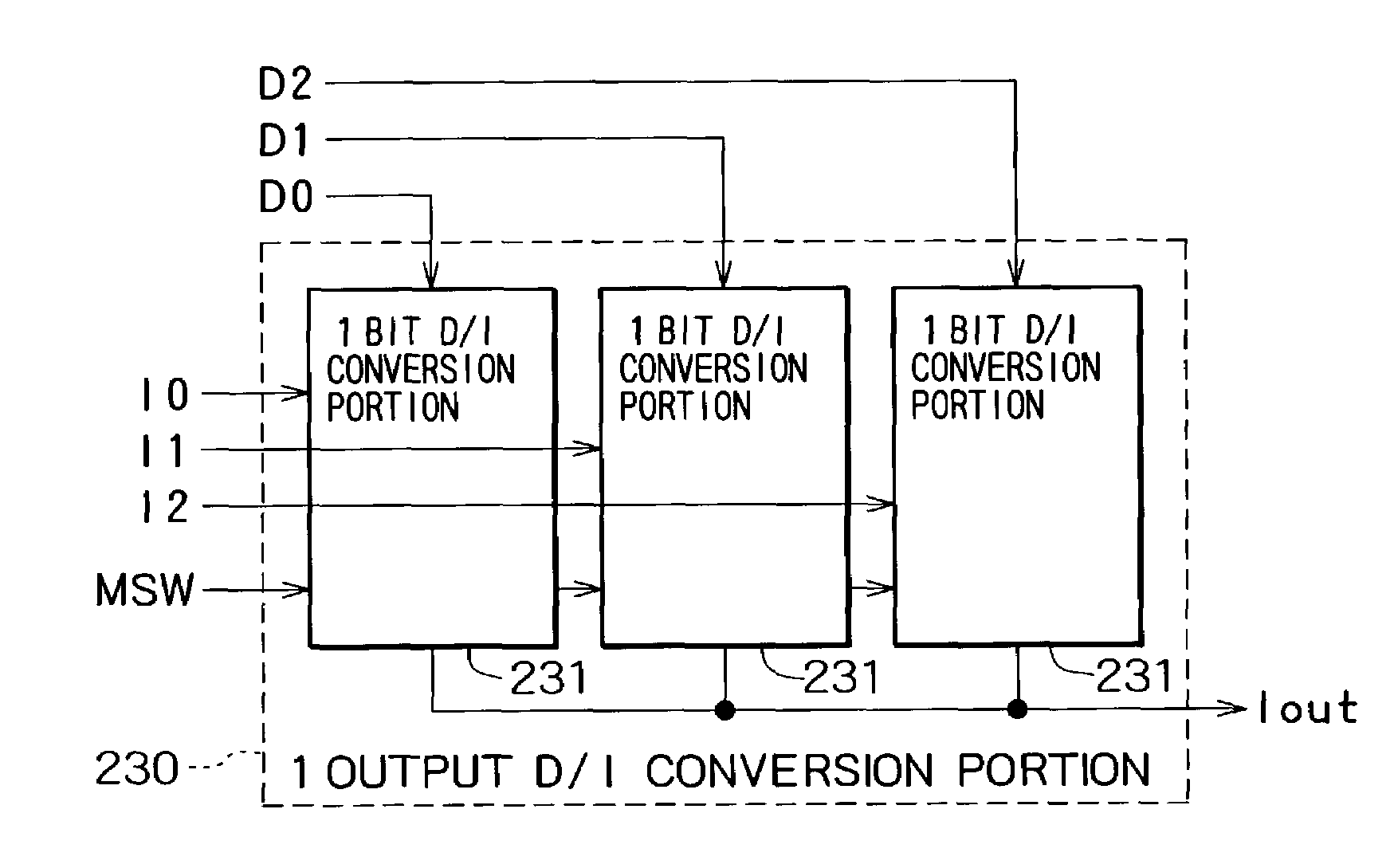
[0144]In the seventh embodiment, a D / I conversion portion 210a is provided, and the D / I conversion portion 210a is provided with a shift register comprising a 1-output D / I conversion portion 230a for the outputs of (3×n) to the light emission display device, and n flip-flops (F / F) 290a_1 to 290a_n provided every 3-output. Into the shift register are input a start signal IST for controlling timing for storing current, a clock signal ICL, an inverted signal ICLB of the clock signal ICL, and a current storing timing signal IT. Further, digital image data D0 to D2 of each output are input into the 1-output D / I conversion portion 230a, and any of reference current IR0 to IR2, IG0 to IG2, and IB0 to IB2 for reference are input according to light emitting colors assigned thereto. One F / F 290a, and three 1-output D / I conversion portions 230a into which are input signals MSW1 and MSW2 output from the F / F 290a constitute one RGB D / I conversion portion 220a.

[0145]FIG. 18 is a block diagram sh...


PUM


Abstract

In a D/I conversion section of the semiconductor device for driving a light emission display device, a precharge circuit is provided at the rear of each 1-output D/I conversion section. A precharge signal PC is input into the precharge circuit. The D/I conversion section has two output blocks internally thereof, and a role for storing and outputting current is changed every frame to enable securing a period for driving a pixel longer. Further, at the time of driving, in the precharge circuit, current driving is carried out after a voltage corresponding to output current has been applied to the pixel, and therefore, the pixel can be driven at high speed. Thereby, output current of high accuracy can be supplied to digital image data to be input, and even where an output current value is low, the current load device can be driven at high speed.

Description

BACKGROUND OF THE INVENTION[0001]1. Technical Field of the Invention[0002]The present invention relates to a semiconductor device for driving a current load device provided with a plurality of cells including a current load element and a current load device provided therewith, and particularly relates to a semiconductor device for driving a current load device for carrying out a gradation display by a current value to which a current load element is supplied and a current load device provided therewith.[0003]2. Description of the Related Art[0004]There has been developed a current load device provided with a plurality of cells, in the form of a matrix, including a current load element of which operation is decided by current supplied. Its application is, for example, a light emission display device in which a current load element is a luminous element, and an organic EL(Electro Luminescence) display device in which an organic EL element is used as a luminous element.[0005]In the fol...

Claims


Application Information

Patent Timeline
IPC IPC(8): G09G3/30G09G5/00G09G3/32G11C5/00G11C7/02H05B44/00
CPCG09G3/3283G09G3/3241G09G3/325G09G2320/0233G09G2310/0248G09G2310/027G09G2310/0297G09G2300/0842
Inventor ABE, KATSUMI
Owner GOLD CHARM LTD
Why Eureka
Try Eureka