
Method and apparatus for reducing power consumption in an integrated circuit chip

a technology of integrated circuits and power consumption, applied in the field of integrated circuit power consumption reduction techniques, can solve the problems of increasing power consumption, increasing power consumption, and increasing the difficulty of reducing so as to reduce power consumption in integrated circuits and optimize the placement of registers

Active Publication Date: 2007-08-14
SYNOPSYS INC
View PDF2 Cites 16 Cited by
  • Summary
  • Abstract
  • Description
  • Claims
  • Application Information

AI Technical Summary

Benefits of technology

This approach effectively decreases net-switching power by up to 80% by optimizing clock wire capacitance and signal wire lengths, while maintaining performance and timing criticality, thus addressing the limitations of existing power reduction techniques.

Problems solved by technology

However, as the clock frequency of these systems increases, power consumption also increases.
In addition to meeting timing and area constraints, power consumption is becoming an important concern for designers of integrated circuits.
Excessive power consumption can cause problems in dissipating heat.
Furthermore, the clock tree has a large load because it drives all of the registers and the clock lines feeding the registers.
As the frequency increases or the capacitance increases, power consumption increases.
This net-switching power can be somewhat mitigated by decreasing the supply voltage, but this technique has limitations because as supply voltage is decreased, the transistors will run out of headroom and noise margin.
A small amount of power consumption within a cell occurs when a temporary short-circuit path between VDD to ground exists.
For instance, when an inverter circuit switches from high-to-low or low-to-high, for a brief time interval during the transition, the pull-up device and the pull-down device are both conducting, which causes the inverter circuit to consume a large amount of power.
However, when these sections of the chip are active, net-switching power is still being consumed.
Even if all of the above-described techniques are used, power consumption still remains a problem.

Method used


Image

  • Method and apparatus for reducing power consumption in an integrated circuit chip
  • Method and apparatus for reducing power consumption in an integrated circuit chip
  • Method and apparatus for reducing power consumption in an integrated circuit chip

Examples


Embodiment Construction

[0031]The following description is presented to enable any person skilled in the art to make and use the invention, and is provided in the context of a particular application and its requirements. Various modifications to the disclosed embodiments will be readily apparent to those skilled in the art, and the general principles defined herein may be applied to other embodiments and applications without departing from the spirit and scope of the present invention. Thus, the present invention is not limited to the embodiments shown, but is to be accorded the widest scope consistent with the principles and features disclosed herein.

Register Clumping

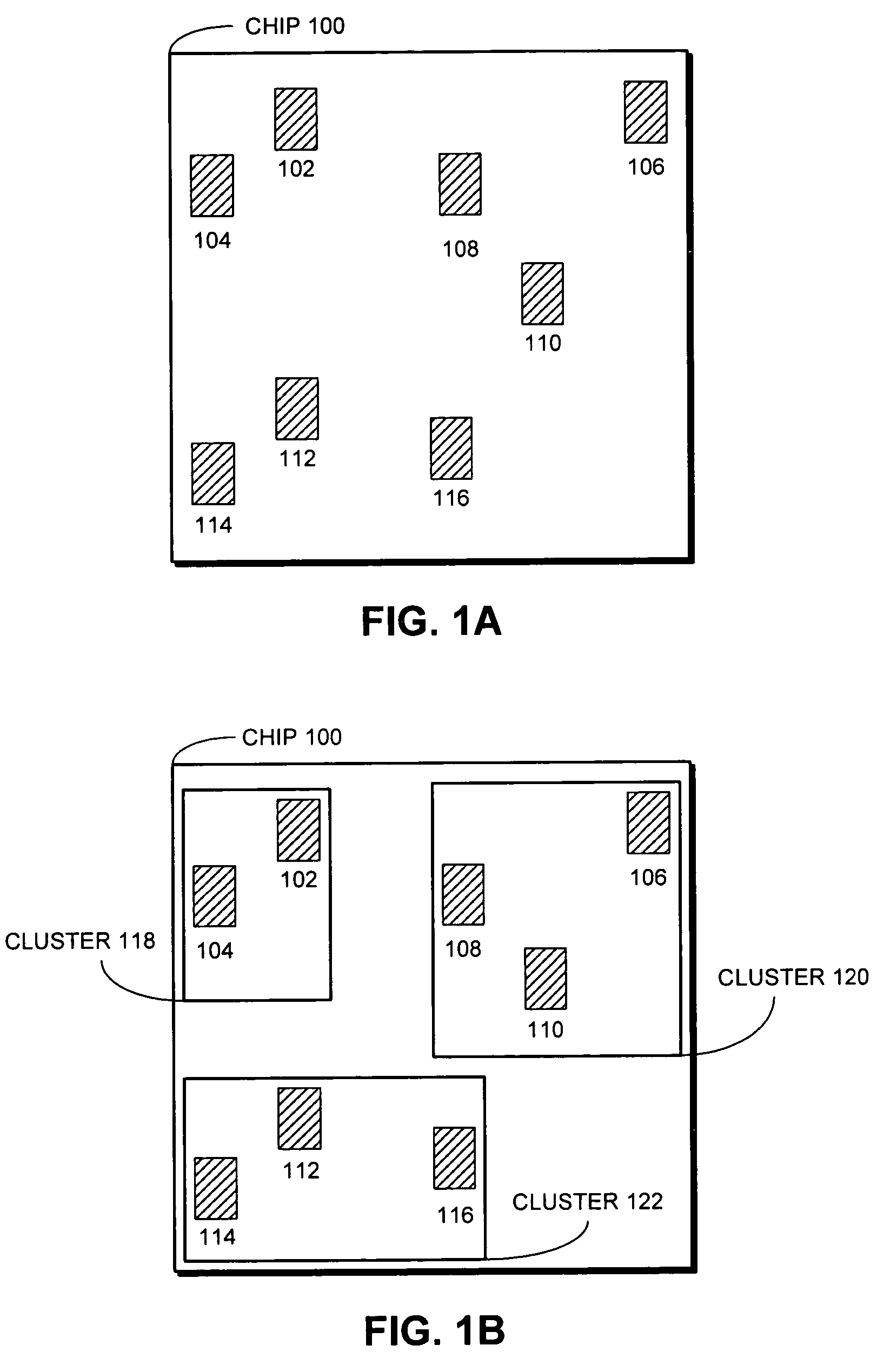
[0032]Up to 80% of the clock wire capacitance is contained within leaf clusters of a clock tree. A leaf cluster in the clock tree contains all of the registers which are connected to a “leaf” clock buffer, which is the farthest clock buffer from the root of the clock tree. Making the leaf clusters smaller decreases the capacitance of the leaf...


PUM


Abstract

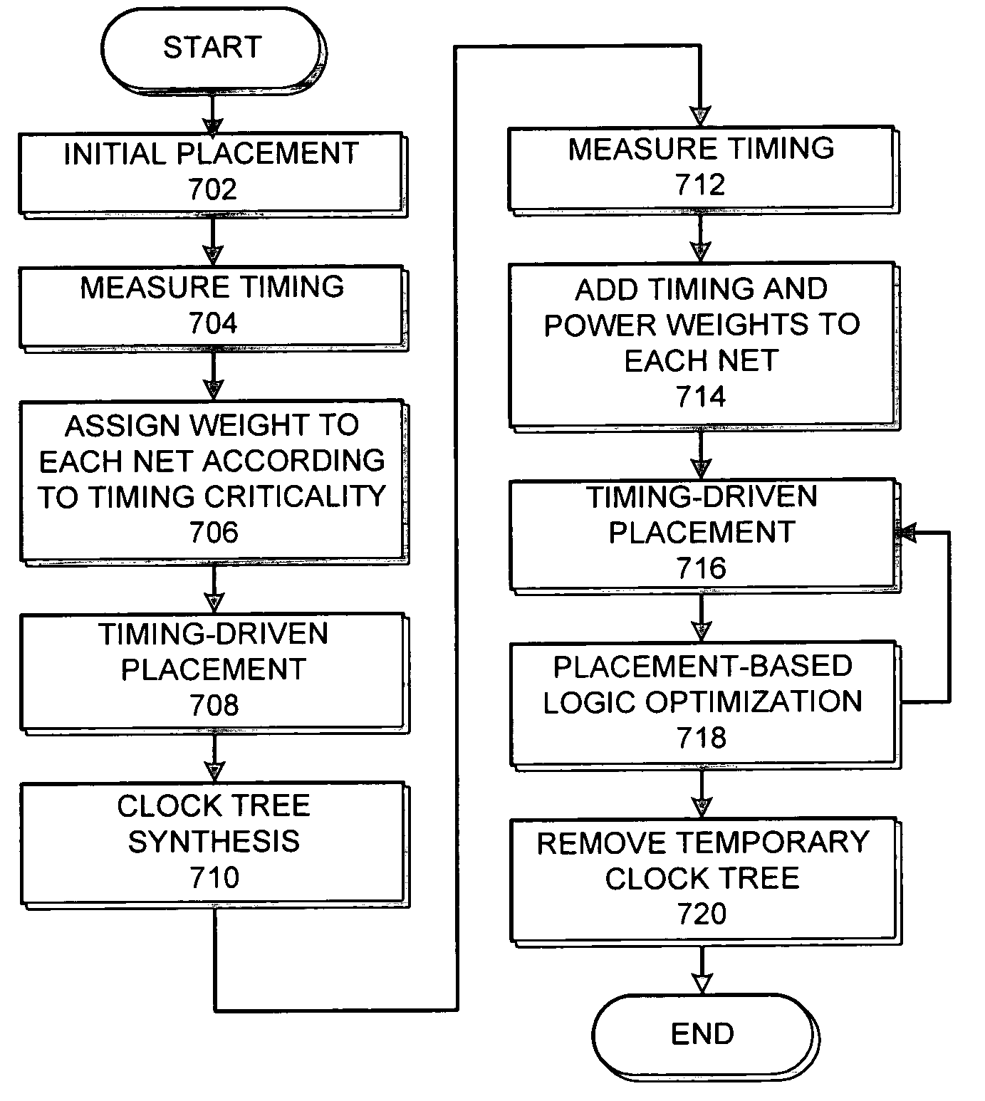
A system that reduces power consumption in an integrated circuit. During operation the system receives a placement for the integrated circuit. The system then groups registers in the placement into clusters and builds a temporary clock tree for the registers within the placement. Next the system assigns net weights to clock wires in the temporary clock tree and signal wires between the rest of the cells of the circuit, and uses the assigned net weights to optimize placement of the cells of the circuit by minimizing a sum of the weighted costs of the wires, wherein the weighted cost of a wire is a product of the net weight of the wire and the length of the wire.

Description

RELATED APPLICATION[0001]This application hereby claims priority under 35 U.S.C. § 119 to U.S. Provisional Patent Application No. 60 / 621,591 filed 22 Oct. 2004, entitled “Low-Power Placement,” by inventors Pei-Hsin Ho, Yongseok Cheon, and Qinke Wang.BACKGROUND[0002]1. Field of the Invention[0003]The present invention relates to techniques for reducing power consumption in an integrated circuit (IC) chip. More specifically, the present invention relates to a method and apparatus for reducing power consumption of the IC chip by judiciously placing the standard cells in the IC chip.[0004]2. Related Art[0005]Advances in semiconductor technology presently make it possible to integrate large-scale systems, including tens of millions of transistors, onto a single semiconductor chip. Integrating such large-scale systems onto a single semiconductor chip increases the speed at which such systems can operate, because signals between system components do not have to cross chip boundaries, and a...

Claims


Application Information

Patent Timeline
Patent Type & Authority Patents(United States)
IPC IPC(8): G06F17/50
CPCG06F17/5072G06F30/392
Inventor HO, PEI-HSINCHEON, YONGSEOKWANG, QINKE
Owner SYNOPSYS INC
Learn More