Active matrix type liquid crystal display device and method of manufacturing the same

a liquid crystal display and active matrix technology, applied in semiconductor devices, semiconductor/solid-state device details, instruments, etc., can solve problems such as leakage of liquid crystal, deterioration of display quality, and electric field caused by data lines, so as to reduce delay of signal and reduce display defects

Inactive Publication Date: 2007-08-21
BEIHAI HKC OPTOELECTRONICS TECH CO LTD
View PDF28 Cites 24 Cited by
  • Summary
  • Abstract
  • Description
  • Claims
  • Application Information

AI Technical Summary

Benefits of technology

[0031]To solve the above problems, an object of the present invention is to provide an active matrix type liquid crystal display device having a lowered delay of a signal and decreased display defects, and a manufacturing method thereof.
[0032]Another object of the present invention is to provide an active matrix type liquid crystal display device which is capable of preventing leakage of an electric field from data lines while lowering delay of a signal, and a manufacturing method thereof.

Problems solved by technology

The so-called leak electric field disturbs the orientation of the liquid crystal 300 and causes disclination, thus display quality is deteriorated.
It is undesirable that the electric field caused by the data lines 106 leaks to the liquid crystal 300.
Thus, the yield is lowered, and the manufacturing cost is increased.
The electrical short circuit increases the possibility that a line defect is caused when the display operation is performed.
However, in such a case where the edge portions of the common electrode are formed so as to overlap a part of the data lines, an electric field leaks to other parts of the unit pixel area than the data lines.
This brings about the same problems as described above.
Thus, to prevent adhesion of ions to the back channel of a TFT, there is a limitation on materials which can be used as the organic film.
Thus, manufacturing steps and manufacturing costs are largely increased.

Method used


Image

  • Active matrix type liquid crystal display device and method of manufacturing the same
  • Active matrix type liquid crystal display device and method of manufacturing the same
  • Active matrix type liquid crystal display device and method of manufacturing the same

Examples


first embodiment

[0126]An active matrix type liquid crystal display device according to a first embodiment of the present invention will now be explained with reference to the drawings. The active matrix type liquid crystal display device according to the first embodiment constitutes an active matrix type liquid crystal display device of an IPS

(In-Plane Switching) mode which uses an electric field formed parallel to the substrate.

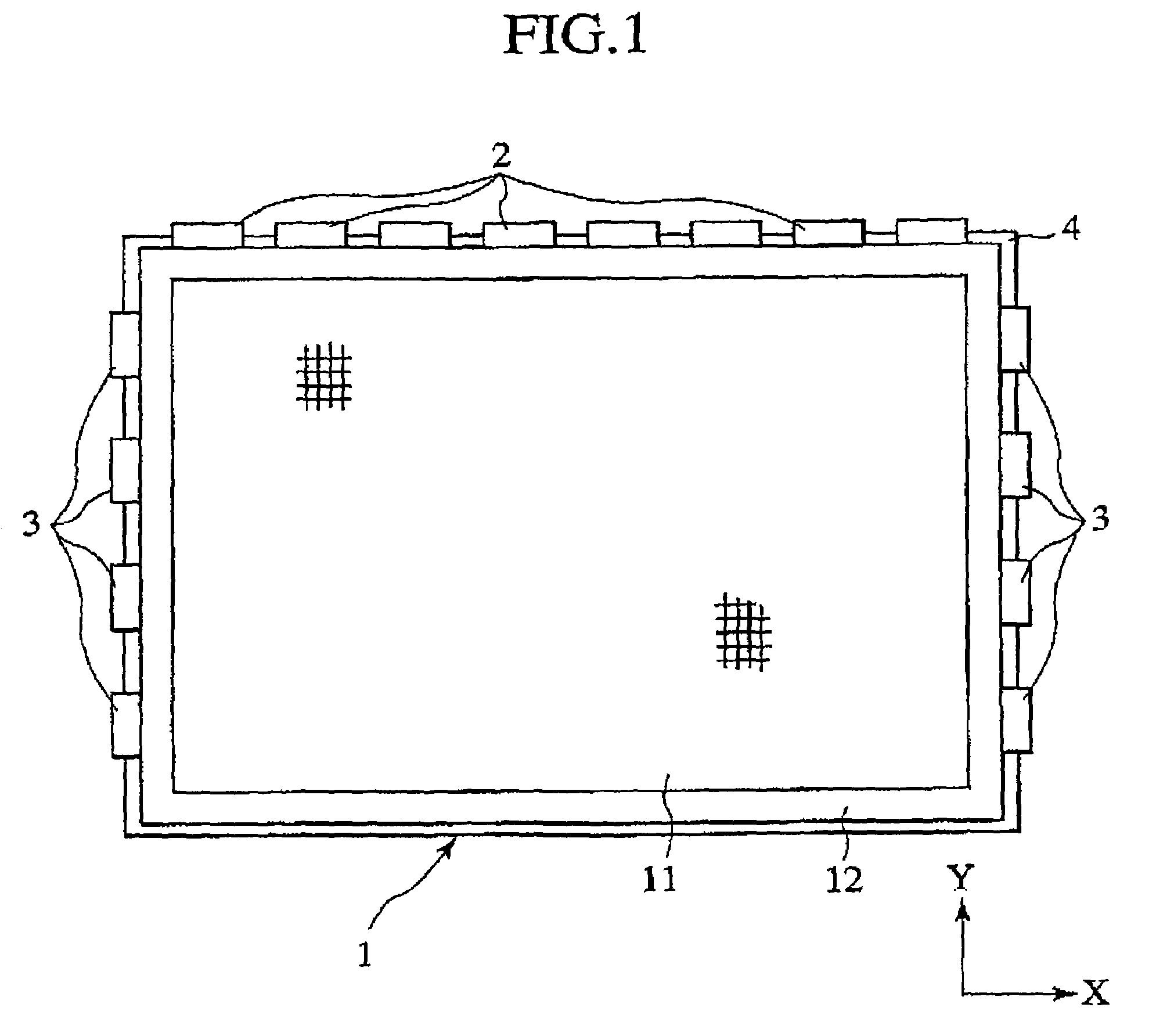
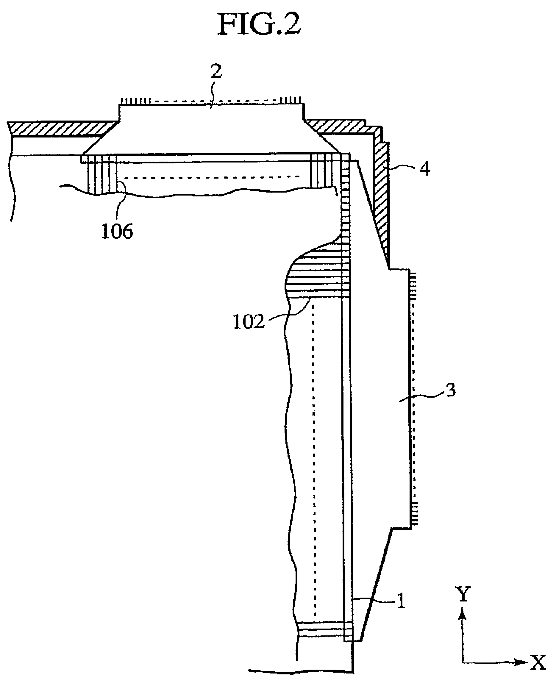
[0127]FIG. 1 shows a plan layout of the whole active matrix type liquid crystal display device according to the first embodiment. FIG. 2 shows an enlarged view of an edge part of the liquid crystal display device 1 shown in FIG. 1. FIG. 3 shows a plan layout of a unit pixel of the liquid crystal display device 1 shown in FIG. 1. FIG. 4 shows a cross section of the unit pixel shown in FIG. 3 as sectioned along a direction A-A.

[0128]As shown in FIG. 1, the liquid crystal display device 1 has almost a rectangular shape. The liquid crystal display device 1 has two parts, a pixe...

second embodiment

[0203]FIG. 10 shows a structure of a liquid crystal display device according to a second embodiment of the present invention. The plan layout of a unit pixel area of the liquid crystal display device according to the second embodiment is identical to the plan layout of the unit pixel area of the first embodiment shown in FIG. 3. Thus, illustration of the plan layout is omitted, and a cross section of the unit pixel area as sectioned along a line corresponding to the line AA of FIG. 3 is shown in FIG. 10. Components identical to those shown in FIG. 3 and FIG. 4 are given the same reference numerals in FIG. 10, and explanation for those components will be omitted.

[0204]As shown in FIG. 10, according to the second embodiment, a connection film 139a is formed on the internal wall of the contact hole 117 for connecting the substrates which is formed in the TFT substrate 100, and on the surface of the common wiring 103 which is exposed at the bottom of the contact hole 117. The connection...

third embodiment

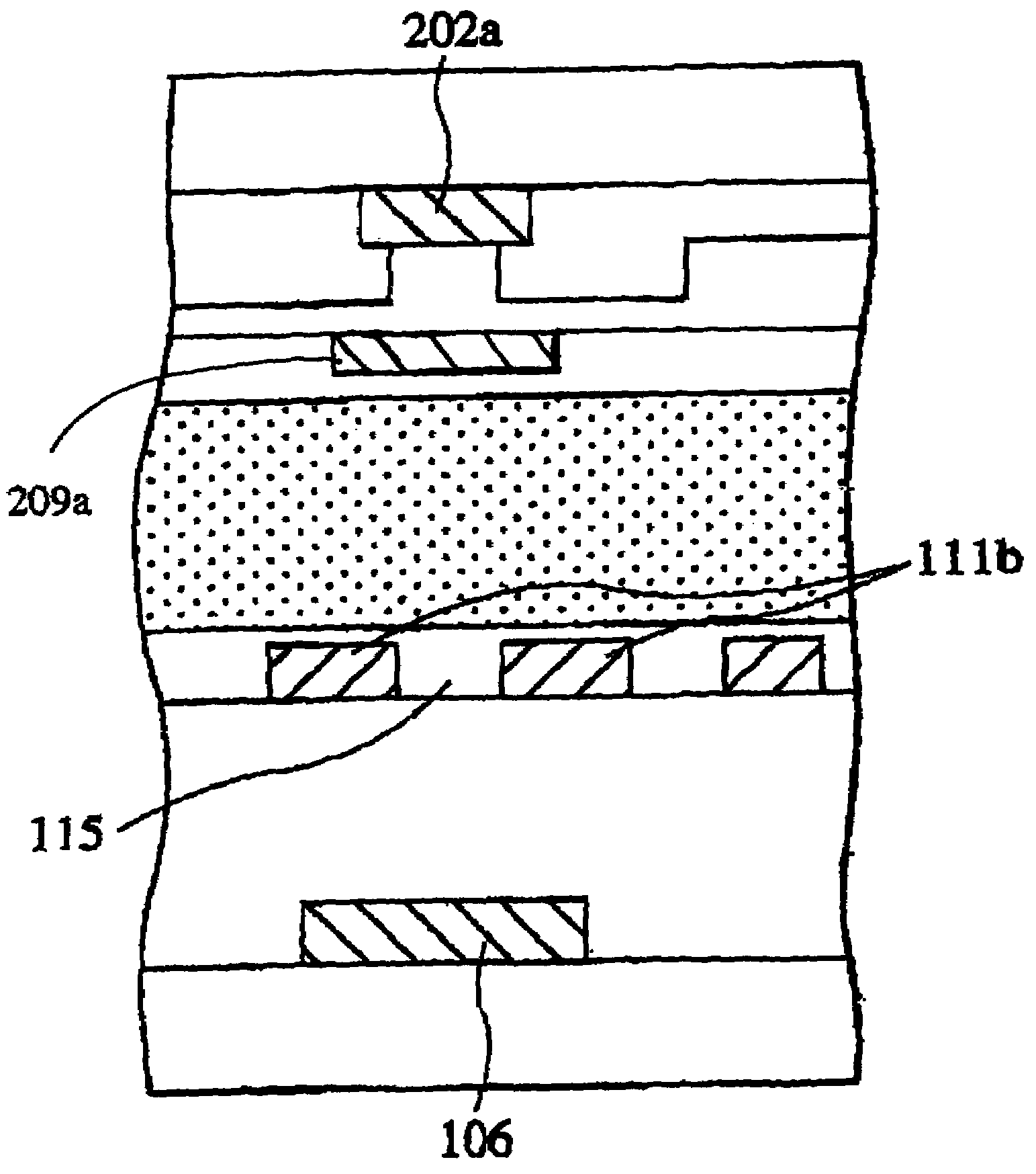
[0209]FIG. 11 shows a structure of a liquid crystal display device according to a third embodiment of the present invention. The plan layout of a unit pixel area of the liquid crystal display device according to the third embodiment is identical to the plan layout of the unit pixel area of the first embodiment shown in FIG. 3. Thus, illustration of the plan layout is omitted, and a cross section of the unit pixel area as sectioned along a line corresponding to the line AA of FIG. 3 is shown in FIG. 11. Components identical to those shown in FIG. 3 and FIG. 4 are given the same reference numerals in FIG. 11, and explanation for those components will be omitted.

[0210]According to the third embodiment, a conductive film for terminating an electric field which leaks through the slit 115 is provided, aside from the black matrix 202.

[0211]As shown in FIG. 11, a conductive film 209 is formed on the flattening film 204 of the opposing substrate 200. The conductive film 209 is made of, for e...


PUM

PropertyMeasurementUnit
thicknessaaaaaaaaaa
widthaaaaaaaaaa
widthaaaaaaaaaa

Abstract

In an active matrix type liquid crystal display device in which a common electrode and a second pixel electrode have portions opposing each other, and an electric field parallel to substrates is formed between the two electrodes, Y direction extending portions of the common electrode are provided above data lines via a second interlayer insulation film. Slits are opened in the Y direction extending portions of the common electrode along the data lines. Portions of a black matrix which are set to a common electric potential with the common electrode are provided on an opposing substrate at positions opposing the slits.

Description

CROSS-REFERENCE TO RELATED PATENT APPLICATION[0001]This application is a division of application Ser. No. 10 / 096,905, filed Mar. 14, 2002 now abandoned, and based on Japanese Patent Application No. 2001-073880, filed Mar. 15, 2001, by Kimikazu Matsumoto. This application claims only subject matter disclosed in the parent application and therefore presents no new matter.BACKGROUND OF THE INVENTION[0002]1. Field of the Invention[0003]The present invention relates to an active matrix type liquid crystal display device having a high performance characteristic and a method of manufacturing the same.[0004]2. Description of the Related Art[0005]There has been developed a so-called In-Plane Switching (IPS) method in which an electric field parallel to a substrate is applied to a liquid crystal for an active matrix type liquid crystal display device. An IPS type liquid crystal display device has such advantages in that a wide angle of view can be obtained.[0006]FIG. 14 shows one example of a...

Claims


Application Information

Patent Timeline
Patent Type & Authority Patents(United States)
IPC IPC(8): G02F1/1343G02F1/1345G02F1/1362G02F1/1368H01L21/3205H01L23/52H01L29/786
CPCG02F1/1345G02F1/134363G02F2001/136218G02F1/136218G02F1/1343
Inventor MATSUMOTO, KIMIKAZU
Owner BEIHAI HKC OPTOELECTRONICS TECH CO LTD
Why Eureka
Try Eureka