Method and system for inspecting a pattern

a pattern and pattern technology, applied in the field of pattern inspection methods, can solve the problems of easy influence of detection and comparison, difficult identification of fine defects, and complicated system construction, and achieve the effects of simple area setting method, high speed, and high reliability

Inactive Publication Date: 2007-08-21
RENESAS TECH CORP
View PDF33 Cites 14 Cited by
  • Summary
  • Abstract
  • Description
  • Claims
  • Application Information

AI Technical Summary

Benefits of technology

[0015]By adopting the detection method and the system construction as described above, for all the areas of the portions which are formed by the small scale repetition of the pattern, any defects can be inspected with high reliability by the simple area setting method.
[0016]In addition, by adopting the above-mentioned system construction, for all the areas of the portions which are formed by the small scale repetition of the pat...

Problems solved by technology

In the conventional first method, two kinds of errors are mixed since the chips have the different patterns as the objects of comparison, and even in the case of the normal portion, the difference occurs so that the identification of the defect of interest to the fine defect becomes difficult.
The first error is due to the object.
The second error is due to the inspection system.
Then, while the patterns are detected and compared with one another after a...

Method used


Image

  • Method and system for inspecting a pattern
  • Method and system for inspecting a pattern
  • Method and system for inspecting a pattern

Examples


first embodiment

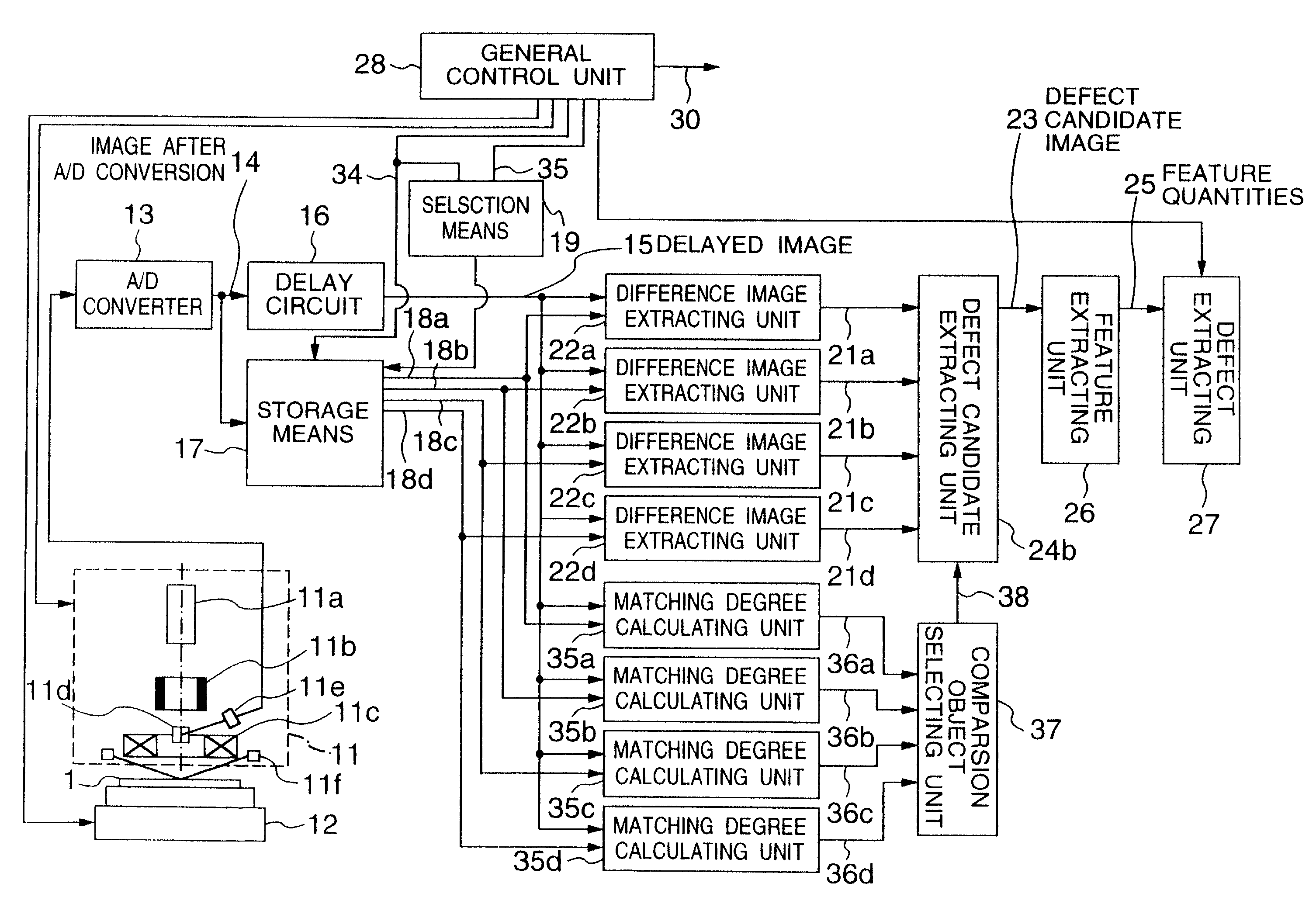
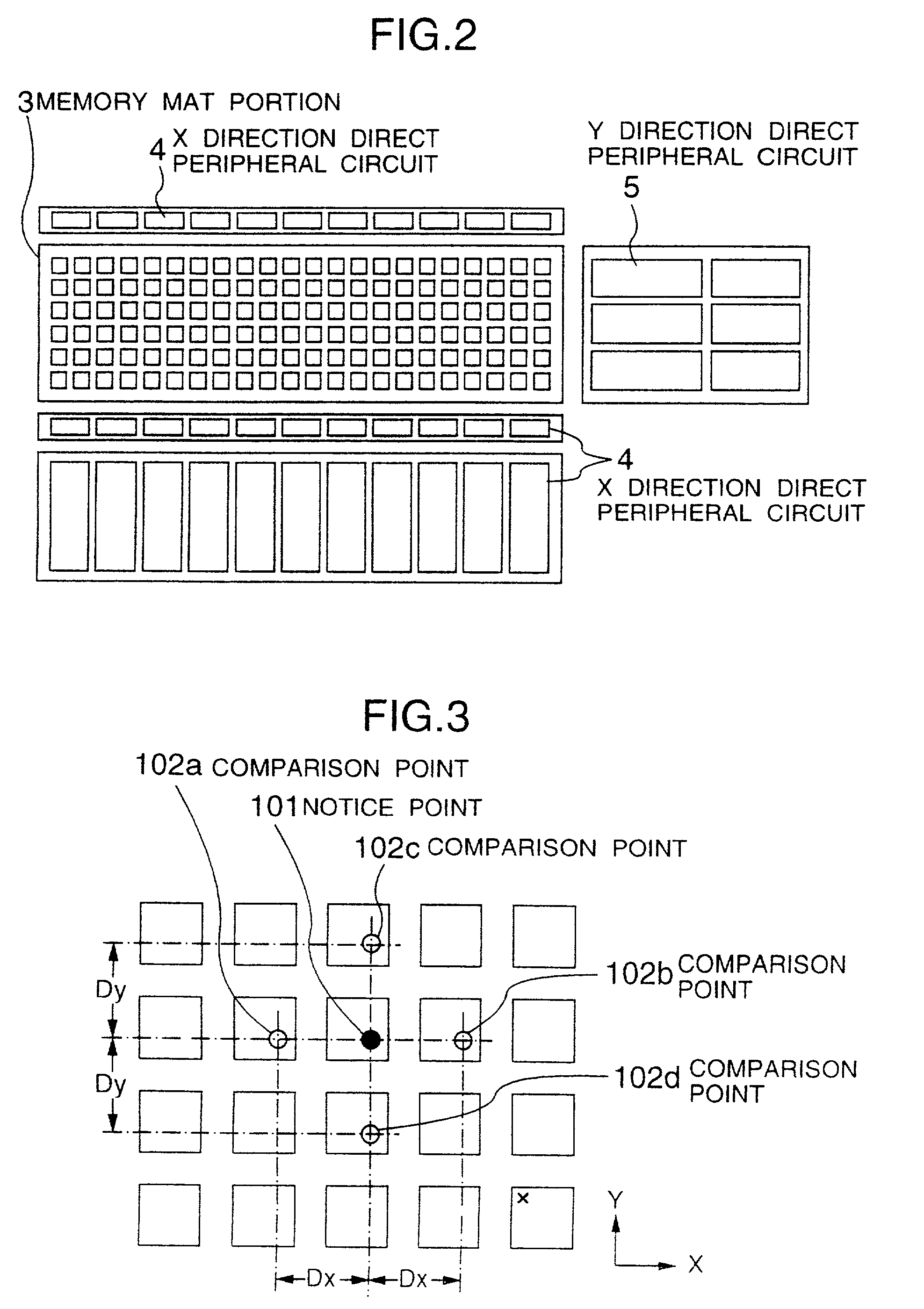
[0061]In a second modification of the first embodiment, instead of the cross-like comparison, as shown in FIG. 12, in addition to the comparison of the pattern of the notice point 101 with the cross-like pattern of the comparison points, the pattern of the notice point 101 is compared with the patterns of two comparison points 102e and 102f arranged in the X direction. This feature is such that it is possible to cope with the case where a plurality of repetitive pitches are present. Likewise, it is considered that a plurality of comparison points are added in each of the X direction and the Y direction. In the case of the second modification, it is necessary to provide additionally difference image extracting units 22e and 22f.

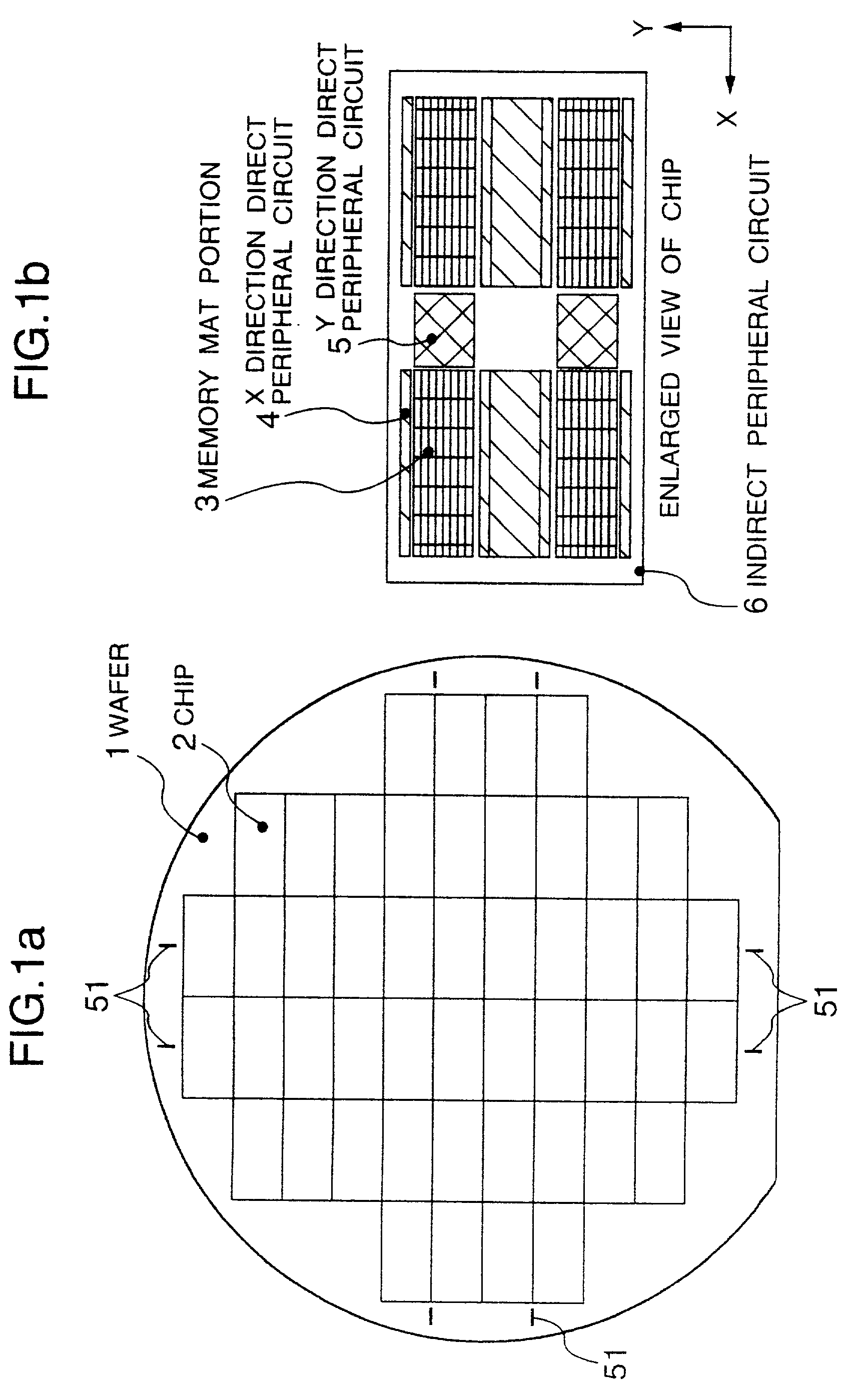
[0062]According to the first embodiment of the present invention as described above, any defect of only the memory mat portion 3 and the direct peripheral circuit 4, 5 each having the repetition and both constituting the semiconductor memory, can be extracted...

fourth embodiment

[0076] since the coordinates of any of the defect candidates are compared with the coordinates which are previously stored, any of the false defects can be surely excluded.

[0077]Naturally, it will be apparent that the fourth embodiment can be applied to the above-mentioned first and second embodiments as well.

[0078]Next, a fifth embodiment of the method and system for inspecting a pattern according to the present invention will hereinafter be described with reference to FIG. 17. FIG. 17 shows the fifth embodiment of the pattern inspection system. A point of difference of the fifth embodiment from the first embodiment is that there are provided: storage means 201 for storing therein the data of the images 14 after the A / D conversion which are used to detect a defect candidate image 206 based on the chip comparison; selection means 202 for fetching selectively the image 207 at a distance backwardly which is integral multiples of the chip, from the images stored in the storage means 20...

fifth embodiment

[0082] the inspection can be carried out with the combination of the cross comparison and the chip comparison, and also any of the defects in the indirect peripheral circuit 6 as well as any of the defects in the memory mat portion 3, the X direction direct peripheral circuit 4 and the Y direction direct peripheral circuit 5, each having the repetition, can be detected.

[0083]Naturally, it will be apparent that the fifth embodiment can be applied to the above-mentioned second, third and fourth embodiments as well.

[0084]While in all the first to fifth embodiments as described above, the description has been given with respect to the case of the system employing the electronic optical detection means, it is to be understood that even in the system employing any of detection means such as optical detection means, all the embodiments can be implemented similarly.

[0085]According to the present invention, by the simple specification of the inspection area, the highly reliable inspection ca...


PUM


Abstract

The present invention relates to detection of defects with simple specification of the coordinates, in the inspection of an object having a plurality of patterns in which a portion having the two-dimensional repetition and portions having the repetition only in the X direction and in the Y direction are mixedly present. The cross comparison between a notice point and comparison points, for example which are repetitive pitches away from the notice point, is carried out, and only the portion having the difference which can be found out with any of the comparison points is extracted as a defect candidate, which results in that the portion having the two-dimensional repetition as well as the portion having the repetition only in the X direction or in the Y direction can be inspected. As a result, while the portion, such as an isolated point, having no repetition both in the X direction and in the Y direction is extracted as the defect candidate, the defect candidate is not treated as the defect in the case where the defect candidate of interest occurs regularly in a plurality of objects to be inspected, so that such a defect candidate is excluded to extract only a true defect.

Description

[0001]This is a continuation application of U.S. Ser. No. 08 / 932,193, filed Sep. 17, 1997.BACKGROUND OF THE INVENTION[0002]The present invention relates to a pattern inspecting method and a system for use in such a method in which an image or a waveform representing the physical properties of an object such as a semiconductor wafer or the like is obtained by utilizing light, an electron beam or the like, and the image or the waveform is compared with the design information or the resultant image, thereby inspecting a pattern, and a semiconductor wafer manufacturing method employing the same.[0003]As for the conventional method of inspecting a pattern, as described in JP-A-6-294750, there is well known a first method wherein by utilizing the property in which it can be expected that the chips adjacent to one another have the same pattern, a pattern of one chip is compared with that of the chip adjacent thereto, and if there is any difference therebetween, then it is judged that the p...

Claims


Application Information

Patent Timeline
IPC IPC(8): G06K9/00G01B11/24G01N21/956G06T1/00G06T7/00H01L21/66
CPCG06T7/001G06T2207/10056G06T2207/30148H01L22/00
Inventor HIROI, TAKASHITANAKA, MAKIWATANABE, MASAHIROKUNI, ASAHIROSHINADA, HIROYUKINOZOE, MARISUGIMOTO, ARITOSHISHISHIDO, CHIE
Owner RENESAS TECH CORP
Why Eureka
Try Eureka