Method and apparatus for estimating parasitic capacitance

a technology of capacitance estimation and parasitic capacitance, applied in the field of process of estimating capacitance in an integrated circuit, can solve the problems of large processing time of 3-d methods, and increased complexity of parametric methods

Active Publication Date: 2007-08-21
SYNOPSYS INC
View PDF15 Cites 15 Cited by
  • Summary
  • Abstract
  • Description
  • Claims
  • Application Information

AI Technical Summary

Benefits of technology

[0017]In a variation on this embodiment, the three-dimensional layout of the integrated circuit is represented using an oct-tree variant that only allows two-way node splits, thereby facilitating efficient execution of geometric queries without using a large amount of storage space.
[0024]In a variation on this embodiment, the system pre-computes Green's functions for the identified dielectric configurations. The system also computes various multiple dielectric configurations at plurality of locations in the design. Green's functions are also computed for these dielectric configurations. Next, the system archives this set of computed Green's functions by storing them in a library, thereby allowing a capacitance estimation process to quickly lookup the value of a Green's function that corresponds to the fabrication technology.

Problems solved by technology

Parasitic capacitances, which could previously be extracted using simplified methods, are now more difficult to compute because of the increased effect of fringe capacitances at small dimensions.
Moreover, since miniaturization is expected to continue, accurate estimation of parasitic capacitance is expected to become even more critical in the future.
However, it is well known that 3-D methods require large processing times and many of these methods do not scale well.
Even though this approach reduces the size of the resultant linear systems, they still result in large linear systems.
Both FEMs and BEMs are computationally infeasible to solve for large integrated circuits.
Still these methods are infeasible to solve large integrated circuits.
Unfortunately, present statistical methods for estimating capacitances suffer from two main drawbacks.
First, present statistical methods tend to be inefficient if the integrated circuit contains multiple layers of dielectrics.
Hence, it is not practical to use existing statistical methods to estimate capacitance.
Second, existing statistical methods have slower convergence properties and tend to report capacitance estimates with larger variance in given computation time.
To get capacitance estimates with smaller variance requires large amount of computational time.
Since the subsequent timing or signal integrity analyses is highly sensitive to the accuracy of the estimated capacitance, having a large variance in the estimated capacitance can have a detrimental effect in these subsequent analyses.

Method used


Image

  • Method and apparatus for estimating parasitic capacitance
  • Method and apparatus for estimating parasitic capacitance
  • Method and apparatus for estimating parasitic capacitance

Examples


Embodiment Construction

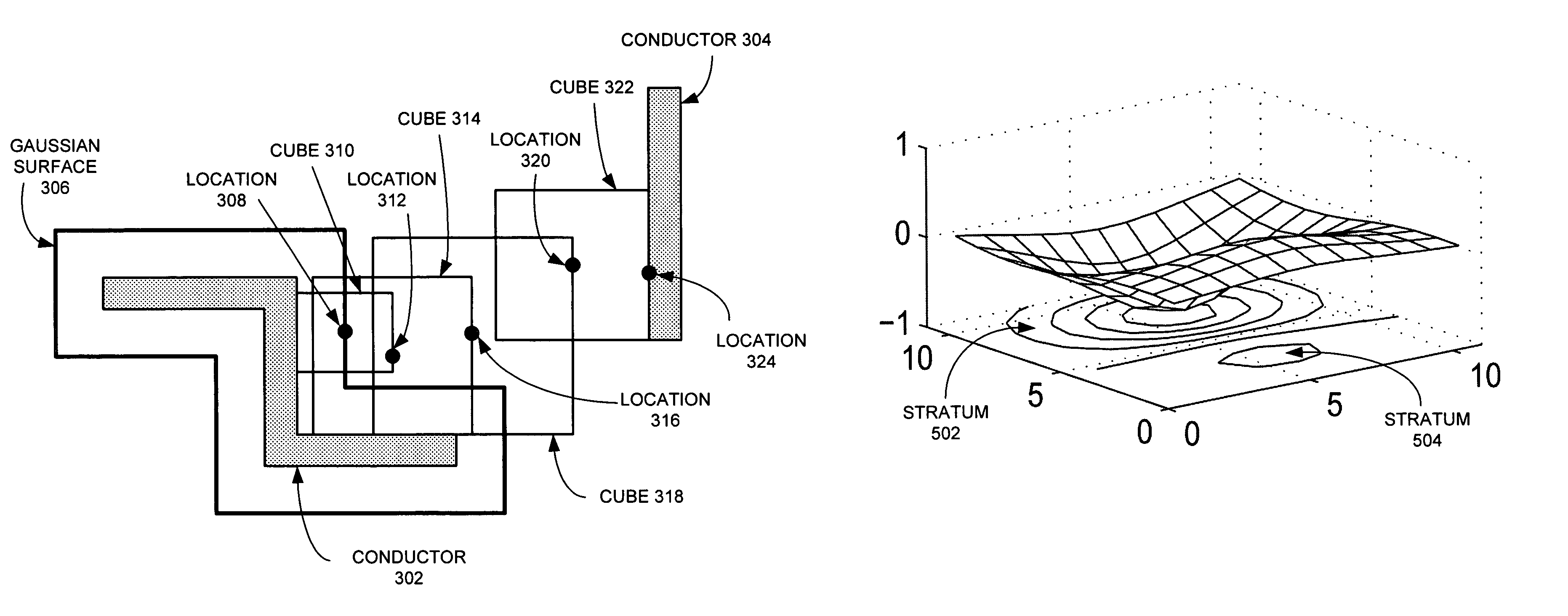
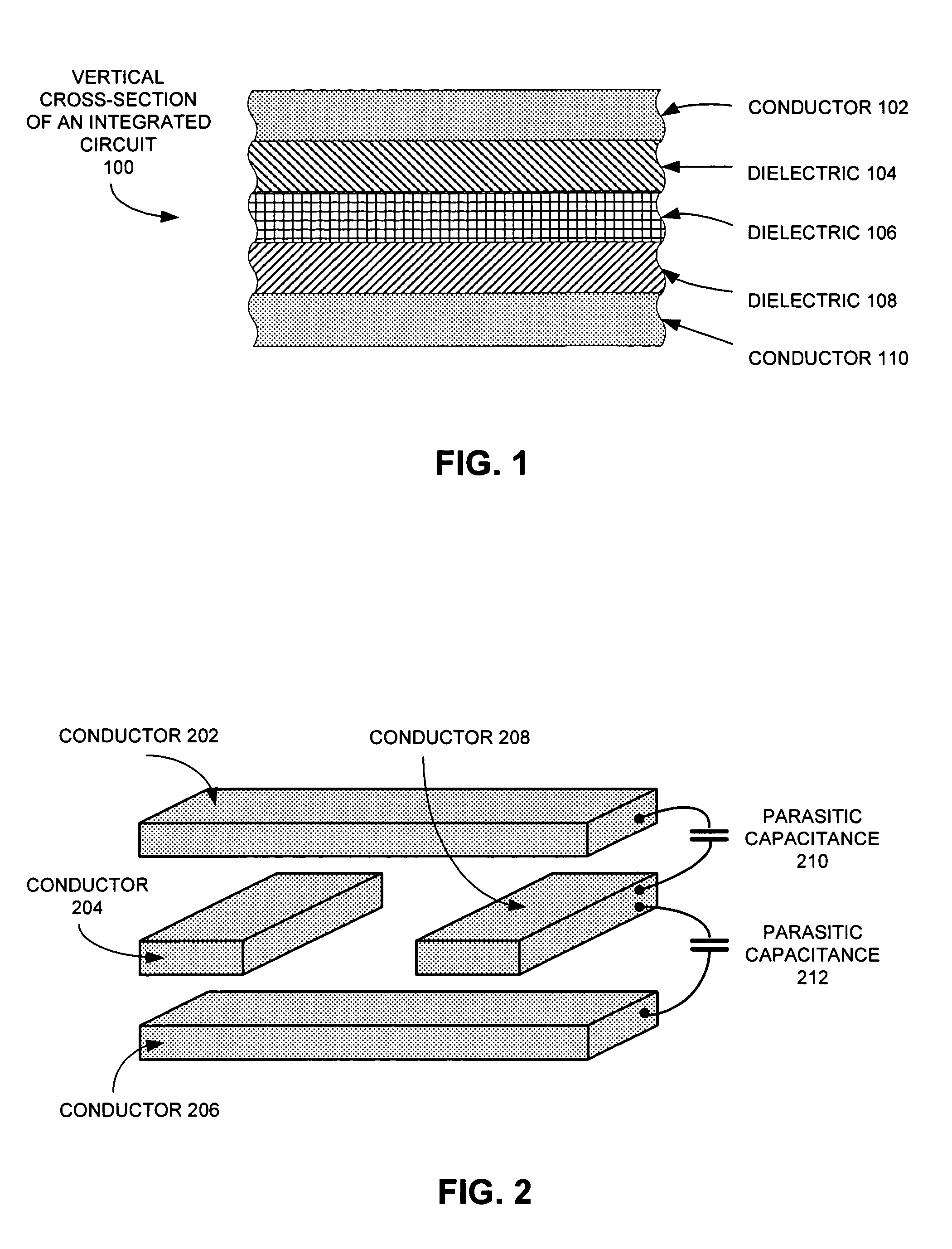
Vertical Cross-Section of an Integrated Circuit

[0034]FIG. 1 illustrates the composition of a vertical cross-section of an integrated circuit 100 in accordance with an embodiment of the present invention.

[0035]Integrated circuit fabrication is a complex multiple-step sequence of predominantly chemical processing steps. Some of the chemical processing steps result in adding a layer of dielectric material to the composition of the integrated circuit. In today's processing technology, it is common to have three or more layers of dielectric material between the conductor layers.

[0036]Specifically, the processing steps can be grouped into two categories, namely, front-end processing steps and back-end processing steps.

[0037]Front-end processing steps typically involve preparation of the wafer surface, patterning and subsequent implantation of dopants to obtain the desired electrical properties, deposition of a gate dielectric, and deposition of insulating materials to isolate neighboring ...


PUM


Abstract

One embodiment of the present invention provides a system for estimating parasitic capacitance for an integrated circuit. During operation, the system reads a technology file, which describes the composition of a vertical cross-section of the integrated circuit. Next, the system reads a design file, which specifies the layout of the integrated circuit. The system then identifies a set of dielectric configurations based on information contained in the technology file. It then computes Green's function for each of these configurations. Next, the system estimates a parasitic capacitance using information contained in the design file and using the set of Green's functions.

Description

BACKGROUND[0001]1. Field of the Invention[0002]The present invention relates to the process of estimating capacitance in an integrated circuit. More specifically, the present invention relates to the process of estimating parasitic capacitance in an integrated circuit by using a set of Green's functions.[0003]2. Related Art[0004]Throughout recent history, the relentless miniaturization of integrated circuits has been a key driving force behind technological innovation. Today, integrated circuits are being built at deep sub-micron (DSM) dimensions. At these dimensions, accurate estimation of parasitic capacitances has become absolutely critical for performing any subsequent timing or signal integrity analyses.[0005]Parasitic capacitances, which could previously be extracted using simplified methods, are now more difficult to compute because of the increased effect of fringe capacitances at small dimensions. Moreover, since miniaturization is expected to continue, accurate estimation ...

Claims


Application Information

Patent Timeline
Patent Type & Authority Patents(United States)
IPC IPC(8): G06F9/45G06F17/10G06G7/56
CPCG06F17/5081G06F30/398
Inventor BATTERYWALA, SHABBIR H.SHENOY, NARENDRADESAI, MADHAV
Owner SYNOPSYS INC
Why Eureka
Try Eureka