Optical connection block, optical module, and optical axis alignment method using the same

a technology of optical connection block and optical module, applied in the field of optical modules, can solve the problems of difficult manufacturing, communication device connected by copper line, inconvenient high-speed pcbs, etc., and achieve the effect of improving optical axis alignment and being easy to manufactur

Inactive Publication Date: 2007-08-28
SAMSUNG ELECTRONICS CO LTD
View PDF26 Cites 59 Cited by
  • Summary
  • Abstract
  • Description
  • Claims
  • Application Information

AI Technical Summary

Benefits of technology

[0017]One aspect of the present invention relates to an optical module that improves optical axis alignment. Another aspect of the invention relates to optical module that is easier to manufacture, as compared to the conventional devices described above.

Problems solved by technology

However, such PCBs are not suitable for high-speed, long-distance, communication devices.
More specifically, communication devices connected by copper lines cannot easily transmit data with a high transmission rate of a few Gb / sec or more, even at short distances of tens of centimeters, due to high loss rate and noise generation.
However, conventional optical connection blocks have a problem in that they are difficult to manufacture.
More specifically, it is difficult to process an end of the blocks in such a manner that it has an end surface slanted with a predetermined angle.
If the angle of the processed end surface varies, the path of optical signals is changed, and noise and intensity loss occur.
In addition, conventional optical connection blocks have a bulky structure because the optical modules are integrated with optical fibers.
This limits the application of the blocks to optical modules or optical communication systems that require a compact size.

Method used


Image

  • Optical connection block, optical module, and optical axis alignment method using the same
  • Optical connection block, optical module, and optical axis alignment method using the same
  • Optical connection block, optical module, and optical axis alignment method using the same

Examples


fourth embodiment

[0050]FIG. 4A shows an optical module including an optical connection block according to the present invention. FIG. 4B is a sectional view of the structure of a planar optical waveguide shown in FIG. 4a taken along line A-A′. Referring to FIGS. 4A and 4B, an optical module 400 includes a substrate 401, a planar optical waveguide 410 formed on the substrate 401, at least one PCB, and a plurality of optical connection blocks 420a and 420b.

[0051]The planar optical waveguide 410 may be created on the substrate 401 by a semiconductor process. and the planar optical waveguide 410 includes a plurality of waveguides 412 and a plurality of grooves 410a and 410b. The planar optical waveguide 410 has a lower clad 411, a core (not shown), and an upper clad 413 that may be successively laminated on the substrate 401. More specifically, after a lower clad 411 and a core layer are successively laminated on the substrate 401, the core layer is processed by an etching process to form a plurality o...

fifth embodiment

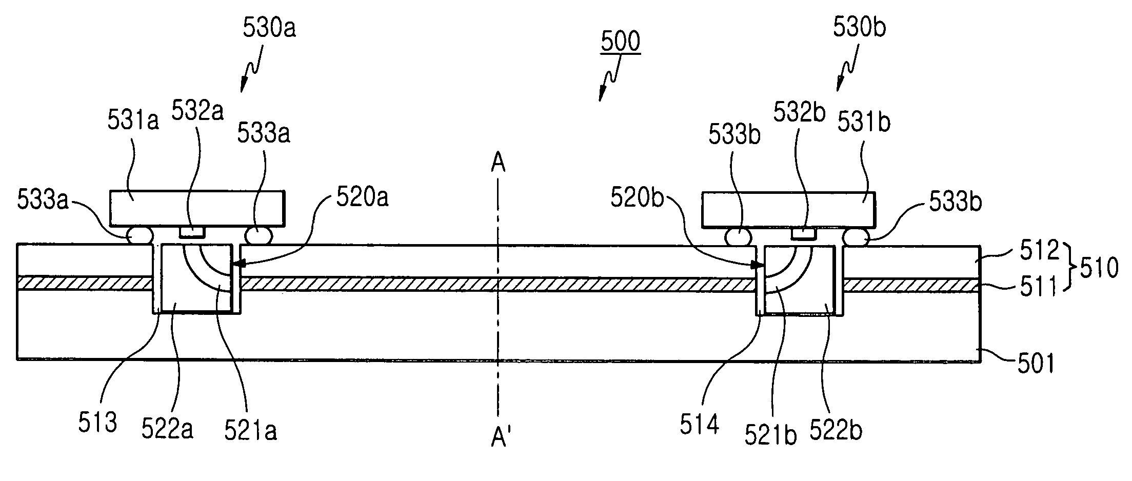
[0065]FIG. 5 shows an optical module including an optical connection block according to the present invention. FIG. 6 is a sectional view showing the structure of a planar optical waveguide shown in FIG. 5. Referring to FIG. 5, an optical module 500 includes a substrate 501, an optical fiber block 510 formed on the substrate 501, at least one PCB 530a and 530b, and a plurality of optical connection blocks 520a and 520b. The substrate 501 has a plurality of V-grooves formed on the upper surface thereof.

[0066]Referring to FIG. 6, which is a sectional view taken along line A-A′ of FIG. 5, the optical fiber block 510 includes a plurality of first optical fibers 511 seated on the respective V-grooves of the substrate 501 and an upper block 512 for covering the substrate 501, on which the first optical fibers 511 are seated. The upper block 512 has a plurality of V-grooves (not shown) for holding the first optical fibers 511 in a stable manner.

second embodiment

[0067]The construction of the optical module 500 is the same as that of the present invention, and repeated descriptions thereof will be omitted.


PUM


Abstract

An optical module is disclosed. The optical module includes a substrate, and at least one planar optical waveguide that includes a plurality of waveguides and at least one groove vertically penetrating the upper surface of the substrate and which is successively laminated on the substrate. The optical module also includes at least one PCB having at least one integrated photoelectric conversion device that is positioned on the planar optical waveguide facing a corresponding groove, and at least one optical connection block including a body and optical fibers embedded in the body in such a manner that both ends thereof are exposed to the lateral and upper surfaces of the body. The optical connection block is inserted into the corresponding groove of the planar optical waveguide in such a manner that both ends of the optical fibers, which have been exposed, face the waveguides and the PCBs, respectively.

Description

CLAIM OF PRIORITY[0001]This application claims priority to an application entitled “optical connection block, optical module, and optical axis alignment method using the same,” filed with the Korean Intellectual Property Office on Apr. 2, 2004 and assigned Ser. No. 2004-22908 and an application filed on Apr. 2, 2004 with the same title and assigned Ser. No. 2004-22909, the contents of which are hereby incorporated by reference.BACKGROUND OF THE INVENTION[0002]1. Field of the Invention[0003]The present invention relates to an optical module, and more particularly to an optical module including a printed circuit board (PCB) having a plurality of integrated photoelectric conversion devices and an optical axis alignment method.[0004]2. Description of the Related Art[0005]In general, PCBs have a structure that include copper wiring laminated on a plastic board made of epoxy resin, polyimide resin, or phenol resin. However, such PCBs are not suitable for high-speed, long-distance, communi...

Claims


Application Information

Patent Timeline
Patent Type & Authority Patents(United States)
IPC IPC(8): G02B6/26G02B6/42G02B6/30G02B6/36G02B6/43
CPCG02B6/421G02B6/4214G02B6/43G02B6/30G02B6/3636G02B6/3652G02B6/3676G02B6/3692
Inventor KIM, DONG-SUPARK, HYO-HUNRHO, BYUNG-SUPCHO, HAN-SEOJUNG, SUN-TAE
Owner SAMSUNG ELECTRONICS CO LTD
Why Eureka
Try Eureka