Epoxy resin composition for semiconductor encapsulation, and semiconductor device using the same

a technology of epoxy resin and semiconductor encapsulation, which is applied in the directions of semiconductor/solid-state device details, transportation and packaging, special tyres, etc., can solve the problems of frequent occurrence of short circuits and drastic solutions, and achieve the ability of semiconductor devices, reduce pitch distance, and prevent short circuits

Active Publication Date: 2007-09-04
NITTO DENKO CORP
View PDF24 Cites 3 Cited by
  • Summary
  • Abstract
  • Description
  • Claims
  • Application Information

AI Technical Summary

Benefits of technology

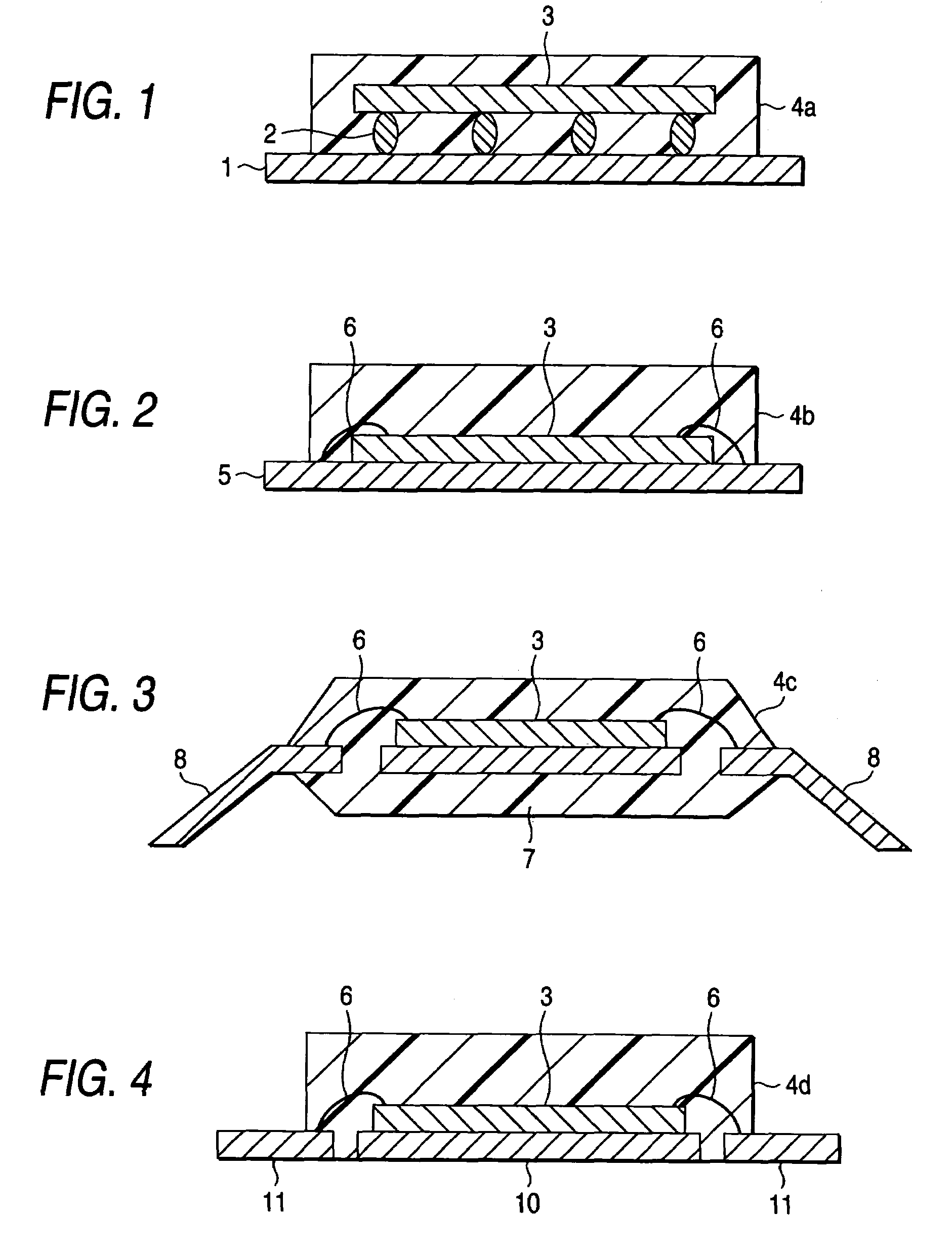
[0004]The capabilities of the semiconductor devices of these types are improving these days, and it is desired to reduce the pitch distance between the interconnection electrodes 2 or the wires 6 in the semiconductor devices. However, the pitch reduction results in frequent occurrence of short circuits in the process of semiconductor encapsulation. In that situation, various investigations are made, for example, for reducing the carbon deposition in semiconductor encapsulation, but could not lead to a drastic solution of the problem. It is now desired to prevent the occurrence of short circuits in producing semiconductor devices, and to produce good semiconductor devices of high reliability.
[0010](C) an inorganic filler capable of preventing semiconductors from short-circuiting in a step of semiconductor encapsulation with the epoxy resin composition.
[0020]Further based on the findings as above, we have made many other studies to find out the uppermost limit of the proportion of carbon-coated inorganic filler particles having a particle size larger than the interconnection electrode or conductor wire distance in semiconductor devices, relative to all the inorganic filler to be used, for preventing the occurrence of short circuits in semiconductor encapsulation. As a result, we have found that, when the proportion of the carbon-coated inorganic filler particles having a particle size larger than the interconnection electrode or conductor wire distance in semiconductor devices is limited to at most 2.5 ppm of all the inorganic filler used for semiconductor encapsulation, then it makes it possible to prevent short circuits in the process of resin encapsulation for producing semiconductor devices.
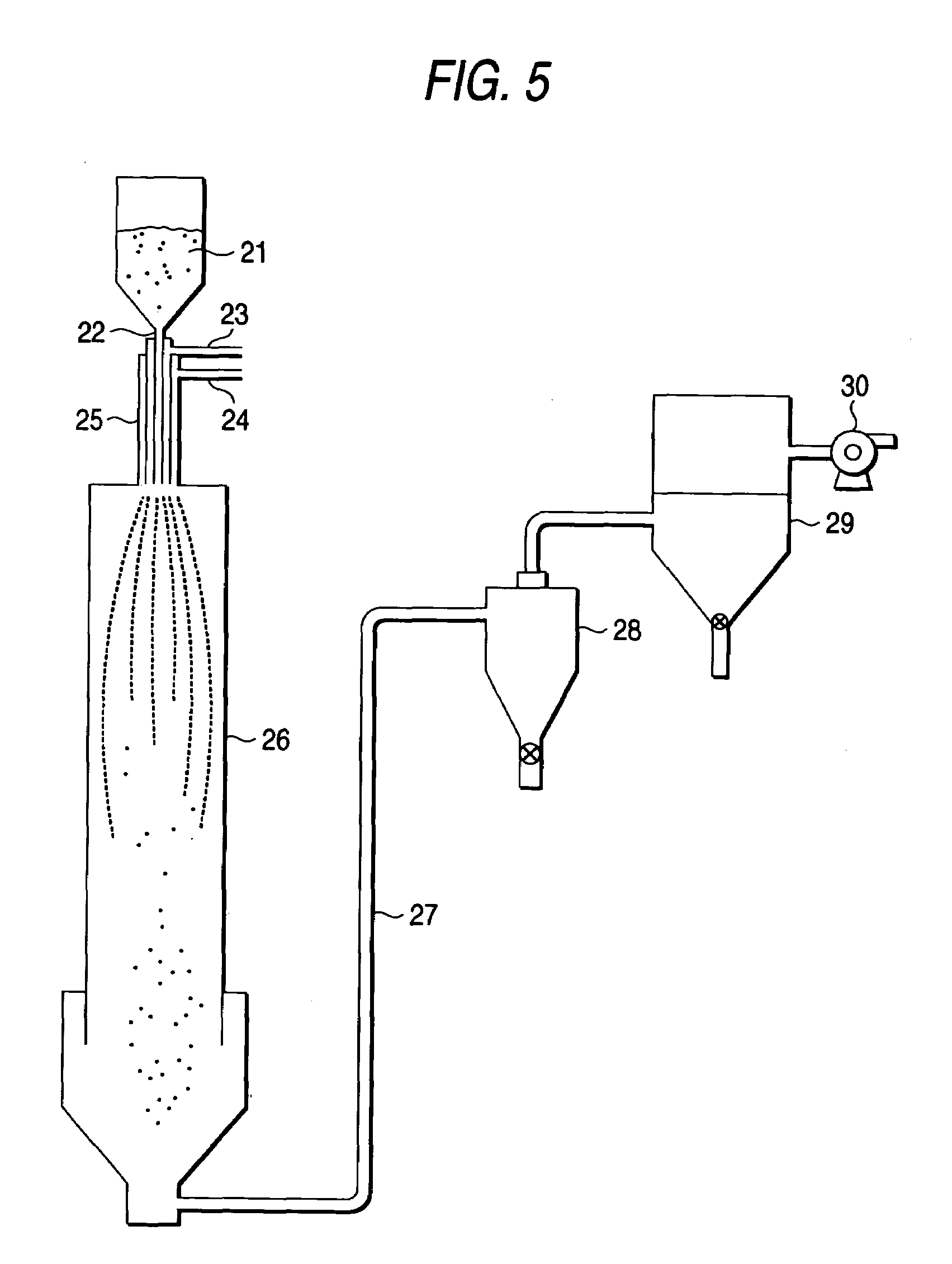
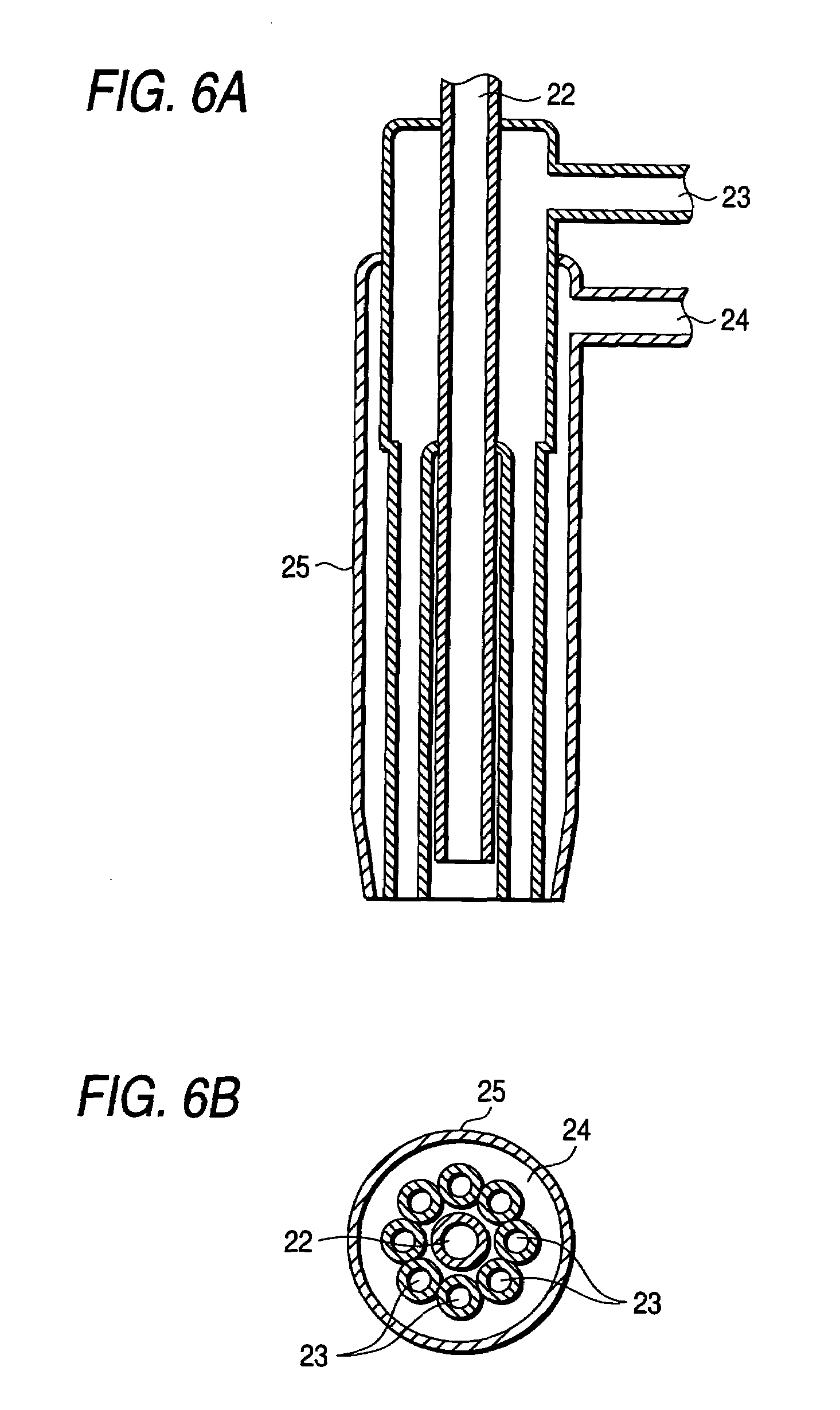
[0021]The present inventors have further found that, when (1) hydrogen gas or (2) a mixture of combustible hydrocarbon gas such as typically propane gas and oxygen gas is used for the heat source for fusion in place of conventional propane gas to produce fused silica particles, then it makes it possible to produce fused silica particles with no carbon deposition around a burner. We have still found that, when an inorganic filler which contains at least 50% by weight of the thus-produced, carbon-uncoated fused silica particles is used in semiconductor encapsulation, then it makes it possible to prevent short circuits in the process of semiconductor encapsulation. On the basis of the findings as above, we have completed the present invention.

Problems solved by technology

However, the pitch reduction results in frequent occurrence of short circuits in the process of semiconductor encapsulation.
In that situation, various investigations are made, for example, for reducing the carbon deposition in semiconductor encapsulation, but could not lead to a drastic solution of the problem.

Method used


Image

  • Epoxy resin composition for semiconductor encapsulation, and semiconductor device using the same
  • Epoxy resin composition for semiconductor encapsulation, and semiconductor device using the same
  • Epoxy resin composition for semiconductor encapsulation, and semiconductor device using the same

Examples


examples b1 to b8

, COMPARATIVE EXAMPLES B1 TO B6, EXAMPLES B1′ TO B8′, COMPARATIVE EXAMPLES B1′ TO B6′, EXAMPLES B1″ TO B8″, COMPARATIVE EXAMPLES B1″ TO B6″

[0129]The components shown in the following Tables 7 to 9, Tables 7′ to 9′ and Tables 7″ to 9″ were put into a Henschel mixer in the ratio also shown in these Tables, and then mixed therein for 30 minutes. In this process, the pigment carbon black was previously mixed with the epoxy resin (b) by the use of a 3-roll mixer (blend ratio of carbon black / epoxy resin (b)=1 / 10 by weight) to prepare a premix, and this was used. Thus prepared, the mixture was fed into a kneading extruder and melt-kneaded through it. Next, the resulting melt was cooled, ground and then tabletted by the use of a tabletting mold into tablets of epoxy resin composition.

[0130]

TABLE 7(parts by weight)Example B123456Epoxy resin (b)303030303030Flame Retardant131313131313Phenol-Novolak Resin555555555555Curing Promoter111111Premix of Carbon777777777777Black / Epoxy Resin (b) (1 / 10)Fl...

examples c1 to c8

, COMPARATIVE EXAMPLES C1 TO C6, EXAMPLES C1′ TO C8′, COMPARATIVE EXAMPLES C1′ TO C6′, EXAMPLES C1″ TO C8″, COMPARATIVE EXAMPLES C1″ TO C6″

[0156]The components shown in the following Tables 13 to 15, Tables 13′ to 15′ and Tables 13″ to 15″ were put into a Henschel mixer in the ratio also shown in these Tables, and then mixed therein for 30 minutes. In this process, the pigment carbon black was previously mixed with the epoxy resin (b) by the use of a 3-roll mixer (blend ratio of carbon black / epoxy resin (b)=1 / 10 by weight) to prepare a premix, and this was used. Thus prepared, the mixture was fed into a kneading extruder and melt-kneaded through it. Next, the resulting melt was cooled, ground and then tabletted by the use of a tabletting mold into tablets of epoxy resin composition.

[0157]

TABLE 13(parts by weight)Example C123456Epoxy resin (b)303030303030Flame Retardant131313131313Phenol-Novolak Resin555555555555Curing Promoter111111Premix of Carbon777777777777Black / Epoxy Resin (b)(1...


PUM

PropertyMeasurementUnit
sizeaaaaaaaaaa
distanceaaaaaaaaaa
mean particle sizeaaaaaaaaaa

Abstract

An epoxy resin composition for semiconductor encapsulation capable of giving semiconductor devices of high reliability that do not cause short circuits even in pitch reduction in the interconnection electrode distance or the conductor wire distance therein as well as a semiconductor device using the same. The epoxy resin composition for semiconductor encapsulation, which comprises the following components (A) to (C): (A) an epoxy resin, (B) a phenolic resin, and (C) an inorganic filler for preventing semiconductors from short-circuiting in a step of semiconductor encapsulation.

Description

FIELD OF THE INVENTION[0001]The present invention relates to an epoxy resin composition for semiconductor encapsulation capable of giving semiconductor devices of high reliability that do not cause short circuits even in pitch reduction in the interconnection electrode distance or the conductor wire distance therein, and relates to the semiconductor device with it.BACKGROUND OF THE INVENTION[0002]Semiconductor chips such as transistors, IC and LSI are generally resin-encapsulated through transfer molding with an epoxy resin composition. Various package forms of the type have heretofore been developed in the art.[0003]One example of the package form is a type as in FIG. 1. In this, 1 is an insulating substrate, and a semiconductor chip 3 is mounted on the insulating substrate 1 via an interconnection electrode 2 so that the insulating substrate 1 and the semiconductor chip 3 are electrically connected to each other. This is encapsulated in an encapsulation resin 4a, a cured product o...

Claims


Application Information

Patent Timeline
Patent Type & Authority Patents(United States)
IPC IPC(8): C08K3/36C08L63/00C08L63/02H01L23/29C08G59/62C08K3/04C08K9/02
CPCC08G59/621H01L23/295C08K3/04C08K3/36C08K9/02H01L2224/48091H01L2224/16H01L2224/48247H01L2224/13H01L2924/00014H01L2224/0401H01L23/29
Inventor AKIZUKI, SHINYAIKEMURA, KAZUHIROITO, HISATAKAUCHIDA, TAKAHIROETO, TAKUYANISHIOKA, TSUTOMUSHIMADA, KATSUMI
Owner NITTO DENKO CORP
Why Eureka
Try Eureka