RF power amplifier having high power-added efficiency

a power amplifier and efficiency technology, applied in the direction of single-ended push-pull amplifiers, modulation, gain control, etc., can solve the problem of not being able to develop only a voltage waveform or a current waveform in a passband (resonant) network, and achieve high output power, high efficiency, and high pae

Inactive Publication Date: 2007-09-04
APPLE INC
View PDF20 Cites 20 Cited by
  • Summary
  • Abstract
  • Description
  • Claims
  • Application Information

AI Technical Summary

Benefits of technology

[0015]The present invention, generally speaking, provides an RF power amplifier that exhibits high PAE at high output powers. The design of the power amplifier is based on the observation that the switching transistor is controlled by either voltage (for a FET) or current (for bipolar transistors), but not both. Thus, it is not necessary to develop power from the driver amplifier in order to operate the final stage as a switch. This recognition runs exactly counter to conventional wisdom, i.e., the concept of impedance matching for interstage design of high efficiency power amplifiers. It is impossible to develop solely a voltage waveform or a current waveform in a passband (resonant) network such as an RF power amplifier—both voltages and current must exist. In accordance with one aspect of the invention, however, instead of ma

Problems solved by technology

It is impossible to develop solely a voltage waveform or a current waveform in a passban

Method used


Image

  • RF power amplifier having high power-added efficiency
  • RF power amplifier having high power-added efficiency
  • RF power amplifier having high power-added efficiency

Examples


Embodiment Construction

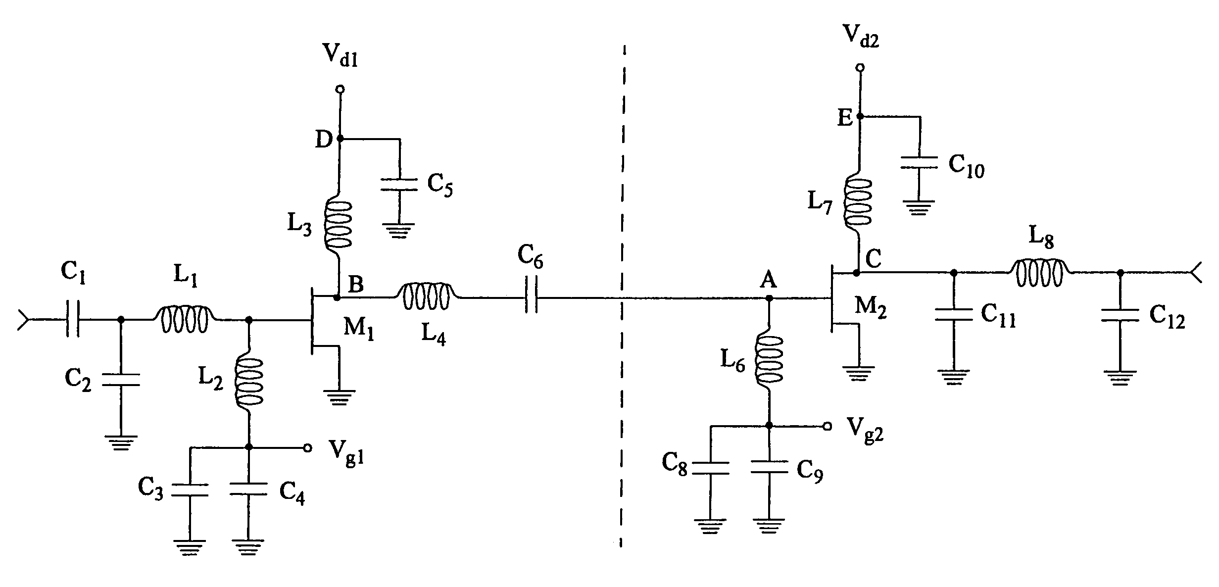
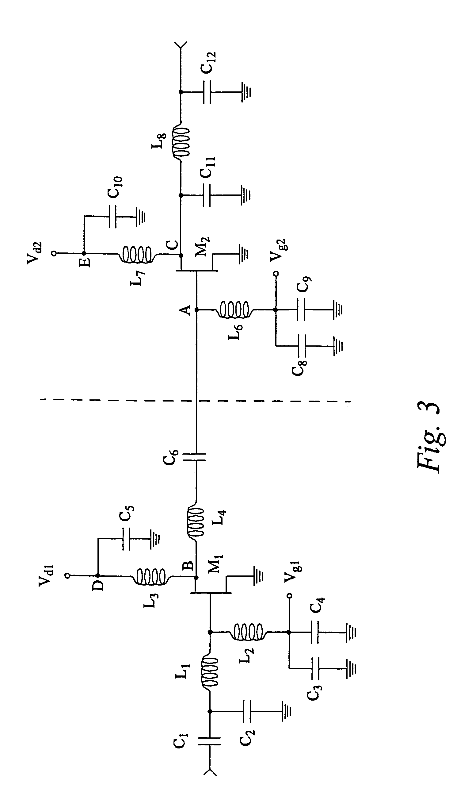
[0021]Referring now to FIG. 3, a schematic diagram is shown of an RF power amplifier circuit in accordance with an exemplary embodiment. An input matching circuit composed of a coupling capacitor C1, a capacitor C2 and an inductor L1 is used to set the input impedance of the circuit. A driver stage M1 and a final stage M2 are shown as FETs, although in other embodiments bipolar transistors may be used. The drain electrode of the FET M1 is coupled to a supply voltage Vd1 through a drain bias network including an RF choke L3 and a capacitor C5. Similarly, the drain electrode of the FET M2 is coupled to a supply voltage Vd2 through a drain bias network including an RF choke L7 and a capacitor C10.

[0022]Respective gate bias networks are provided for the stages M1 and M2. In the case of the stage M1, the gate bias network is composed of an inductor L2, a capacitor C3 and a capacitor C4 connected at a common node to a voltage Vg1. In the case of the stage M2, the gate bias network is comp...


PUM


Abstract

The present invention, generally speaking, provides an RF power amplifier that exhibits high PAE at high output powers. The design of the power amplifier is based on the observation that the switching transistor is controlled by either voltage (for a FET) or current (for bipolar transistors), but not both. Thus, it is not necessary to develop power from the driver amplifier in order to operate the final stage as a switch. This recognition runs exactly counter to conventional wisdom, i.e., the concept of impedance matching for interstage design of high efficiency power amplifiers. It is impossible to develop solely a voltage waveform or a current waveform in a passband (resonant) network such as an RF power amplifier—both voltages and current must exist. In accordance with one aspect of the invention, however, instead of maximizing power transfer, power consumption is reduced while maintaining the magnitude of the voltage (or current) waveform. In accordance with another aspect of the invention, the driver is designed to, along with the final stage, operate in switch mode. In this instance, the design of the interstage network is similar to that of a Class E output stage. In the case of the interstage network, however, the objective is not to develop maximum power across the load (as in the case of the Class E output stage). Rather, the objective is to develop the maximum voltage across the driver's load (which is the switch input). In this arrangement, the input drive of the switch may be sufficiently high that the operating voltage of the driver stage may be reduced. This reduction further reduces the DC supply power to the driver, enhancing PAE.

Description

BACKGROUND OF THE INVENTION[0001]1. Field of the Invention[0002]The present invention relates to RF power amplifiers.[0003]2. State of the Art[0004]Battery life is a significant concern in wireless communications devices such as cellular telephones, pagers, wireless modems, etc. Radio-frequency transmission, especially, consumes considerable power. A contributing factor to such power consumption is inefficient power amplifier operation. A typical RF power amplifier for wireless communications operates with only about 10% efficiency. Clearly, a low-cost technique for significantly boosting amplifier efficiency would satisfy an acute need.[0005]A power amplifier typically includes multiples stages, for example a final output stage and one or more pre-amplifier or driver stages. Much work has been done on maximizing the efficiency of the final output stage. A significant improvement in the efficiency of the final output stage was achieved with the advent of the Class E power amplifier,...

Claims


Application Information

Patent Timeline
IPC IPC(8): H03F3/217H03F3/24H03C5/00H03F1/02H03F3/193H03F3/30H03G3/00
CPCH03C5/00H03F1/0227H03F1/0244H03F1/0261H03F3/193H03G3/004H03F2200/168H03F2200/18H03F2200/504H03F2200/75H03F3/217
Inventor MECK, RONALD A.
Owner APPLE INC
Why Eureka
Try Eureka