4H-SiC metal semiconductor field effect transistor with partial sinking channel

A field-effect transistor and metal-semiconductor technology, applied in the field of 4H-SiC metal-semiconductor field-effect transistors, can solve problems such as performance degradation, affecting device performance, and reducing device frequency characteristics, and achieve improved electric field distribution, high PAE, and increased saturation The effect of current

Pending Publication Date: 2021-12-10
XIDIAN UNIV
View PDF9 Cites 0 Cited by
  • Summary
  • Abstract
  • Description
  • Claims
  • Application Information

AI Technical Summary

Problems solved by technology

[0004] However, the existing improvements have limited improvement in device performance. Many improved structures reduce the breakdown voltage of the device while increasing the transconductance of the device, increase the breakdown voltage of the device and reduce the saturation current of the device, and increase the saturation current of the device while reducing The frequency characteristics of the device, that is, when improving the performance of a certain aspect of the device is often accompanied by a decrease in the performance of a certain aspect
This contradictory relationship seriously affects the improvement of device performance.

Method used


Image

  • 4H-SiC metal semiconductor field effect transistor with partial sinking channel
  • 4H-SiC metal semiconductor field effect transistor with partial sinking channel

Examples


Embodiment 1

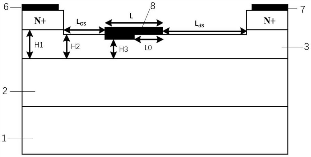
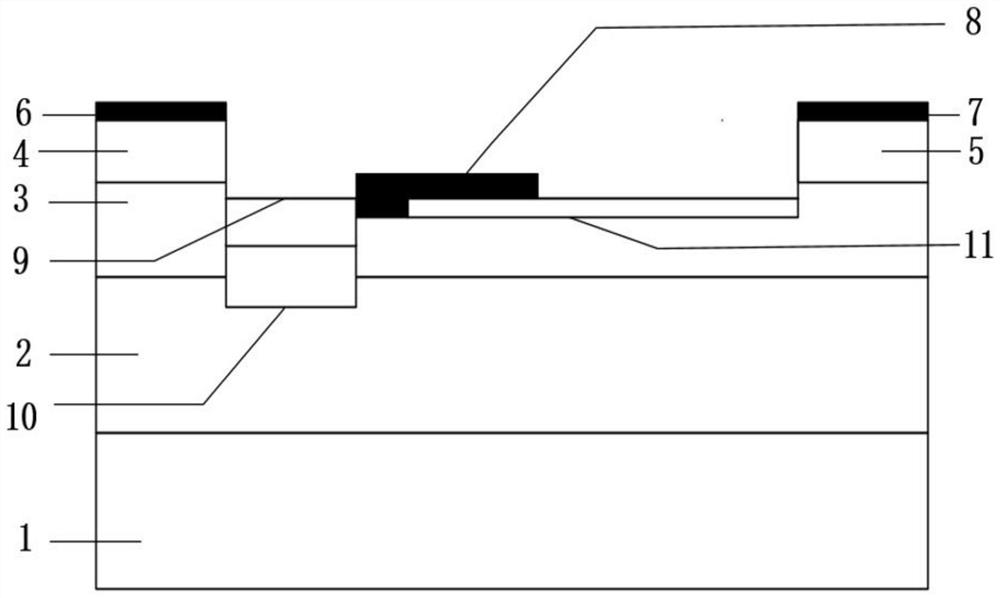
[0024] Such as figure 2 As shown, a 4H-SiC metal-semiconductor field-effect transistor with a partially sunken channel, its structure includes a 4H-SiC semi-insulating substrate 1 from bottom to top, with a width of 0.5 μm and a doping concentration of 1.4×10 15 cm -3 The P-type buffer layer 2 has a width of 0.25 μm and a doping concentration of 3×10 17 cm -3 The N-type channel layer 3, above the N-type channel layer 3 are the source cap layer 4 and the drain cap layer 5 respectively, and the surfaces of the source cap layer 4 and the drain cap layer 5 are respectively the source electrode 6 and the drain electrode 7. A gate electrode 8 is formed on the side close to the source above the N-type channel layer 3, wherein the gate-to-source distance is 0.5 μm, the gate-to-drain distance is 1.0 μm, the gate length is 0.7 μm, and there is a light gap between the gate and the source. The doped region 9, below the lightly doped region is a heavily doped region 10 that partially s...


PUM

PropertyMeasurementUnit
heightaaaaaaaaaa
widthaaaaaaaaaa
heightaaaaaaaaaa

Abstract

The invention relates to the technical field of field effect transistors, and discloses a 4H-SiC metal semiconductor field effect transistor with a partial sinking channel. The 4H-SiC metal semiconductor field effect transistorcomprises a 4H-SiC semi-insulating substrate, a P-type buffer layer and an N-type channel layer from bottom to top, and is characterized in that a source electrode cap layer and a drain electrode cap layer are respectively arranged above the N-type channel layer, a source electrode and a drain electrode are respectively arranged on the surfaces of the source electrode cap layer and the drain electrode cap layer, a gate electrode is formed on one side, close to the source electrode, above the N-type channel layer, a lightly doped region is arranged between the gate electrode and the source electrode, a heavily doped region partially sinking a channel is arranged below the lightly doped region, and an insulating region is arranged between the lower portion of the high gate and the drain electrode. The field effect transistor provided by the invention has high breakdown voltage and can maintain high saturation current and transconductance at the same time, thereby realizing relatively high PAE.

Description

technical field [0001] The invention relates to the technical field of field effect transistors, in particular to a 4H-SiC metal semiconductor field effect transistor with a partially sunken channel. Background technique [0002] The emergence of SiC power devices has greatly improved the performance of semiconductor devices, which is of great significance to the development of the power electronics industry. Compared with Si devices, SiC power devices can effectively realize high efficiency, miniaturization and light weight of power electronic systems. It is understood that the energy loss of SiC power devices is only half that of Si devices, the heat generation is only half that of Si devices, and they have higher current densities. Under the same power level, the volume of SiC power modules is significantly smaller than that of Si power modules. SiC plays a major role in the application of microwave power devices, especially metal-semiconductor field-effect transistors ...

Claims


Application Information

Patent Timeline
Patent Type & Authority Applications(China)
IPC IPC(8): H01L29/06H01L29/10H01L29/786
CPCH01L29/0611H01L29/0649H01L29/0684H01L29/1041H01L29/78696
Inventor 贾护军董梦宇王笑伟朱顺威杨银堂
Owner XIDIAN UNIV
Why Eureka
Try Eureka