Illumination optical system, exposure apparatus, and device manufacturing method with modified illumination generator
a technology of illumination generator and optical system, which is applied in the direction of microlithography exposure apparatus, printers, instruments, etc., can solve the problems of reducing the illumination efficiency of the lens, the inverse proportion of the depth of focus, and the inverse proportion of the dof, so as to achieve the effect of lowering the illumination efficiency
- Summary
- Abstract
- Description
- Claims
- Application Information
AI Technical Summary
Benefits of technology
Problems solved by technology
Method used
Image
Examples
first embodiment
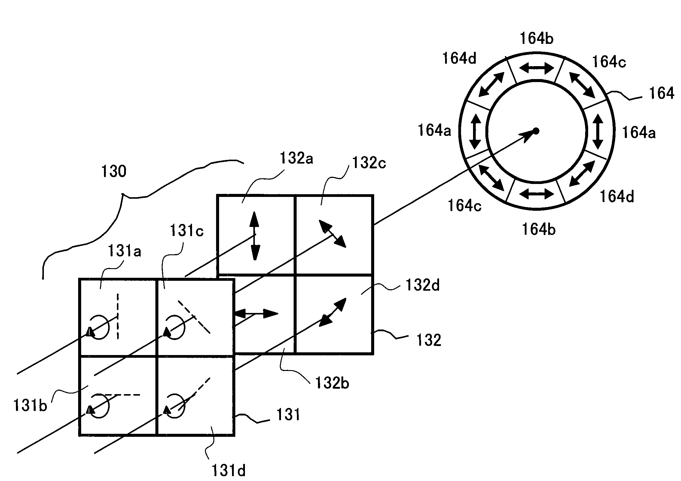
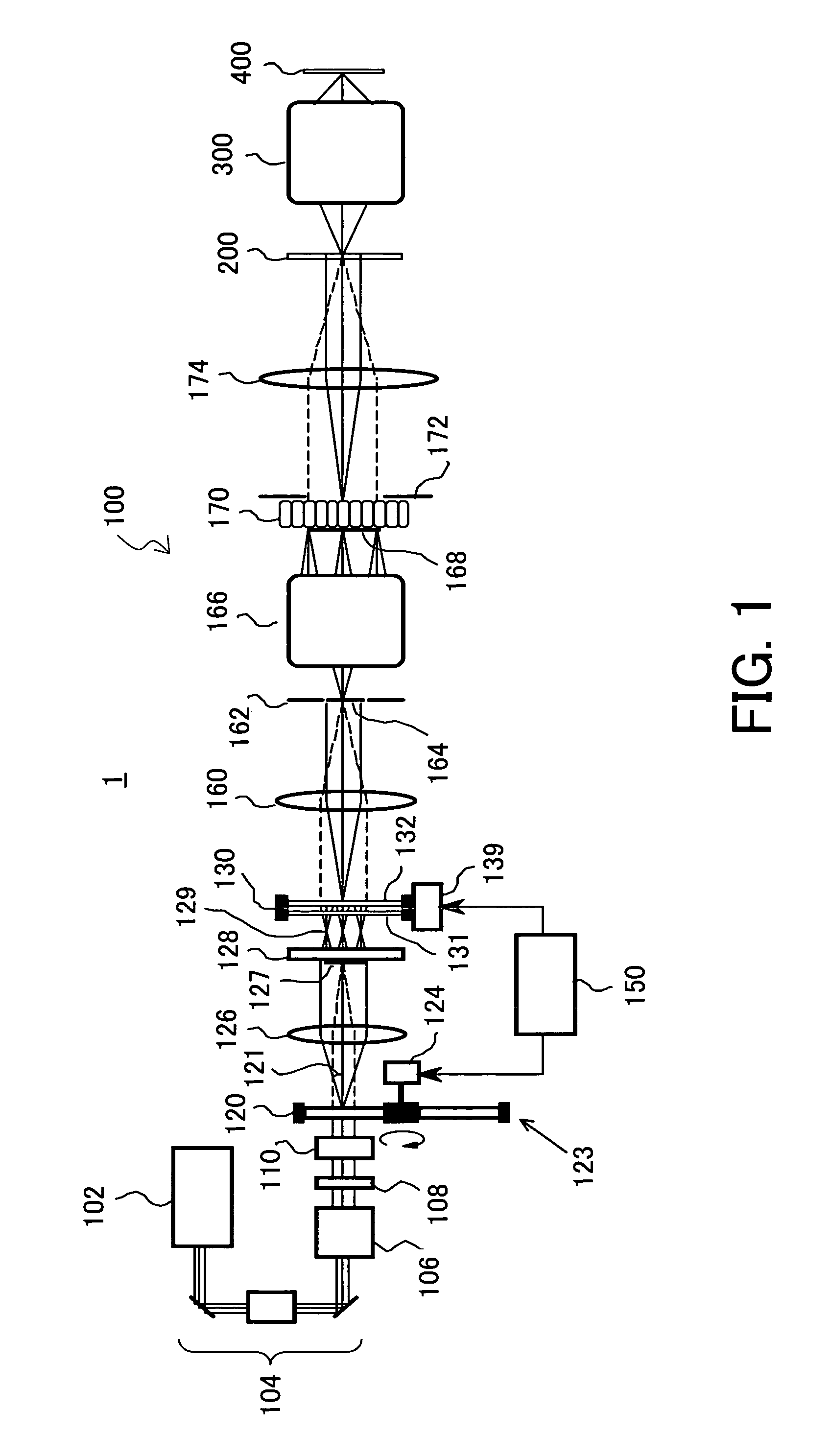
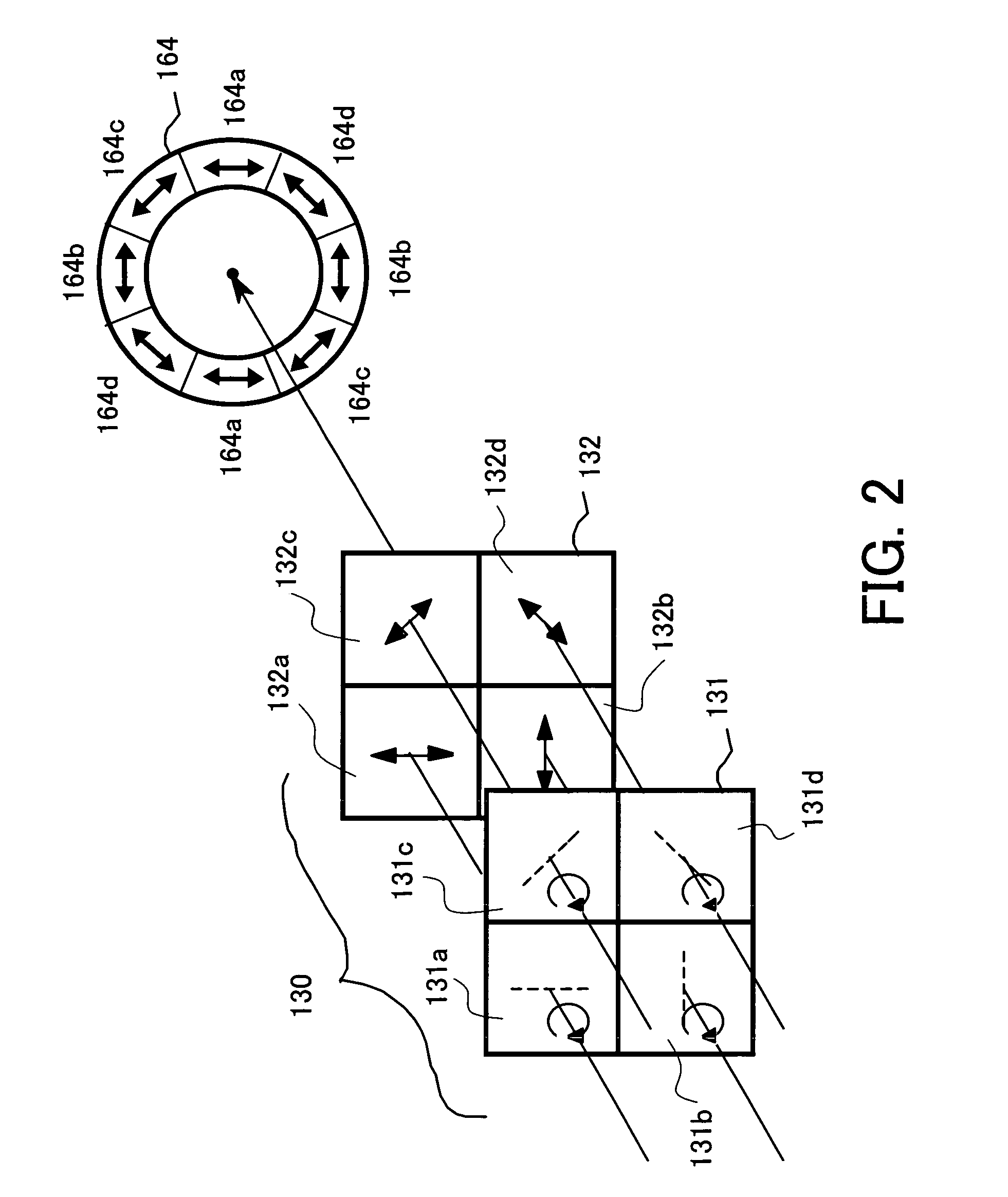
[0036]With reference to the accompanying drawings, a description will now be given of an exposure apparatus 1 having an illumination apparatus 100 according to the present invention. FIG. 1 is a schematic block diagram of the exposure apparatus 1. The exposure apparatus 1 is a step-and-scan projection exposure apparatus (“scanner”) that exposes a circuit pattern of a reticle 200 onto an object (or a plate) 400 in a manner. Of course, the present invention is applicable to a step-and-repeat exposure apparatus (“stepper”). The exposure apparatus 1 is suitable for a sub-micron or quarter-micron lithography process. The “step-and-scan manner”, as used herein, is an exposure method that exposes a reticle pattern onto a wafer by continuously scanning the wafer relative to the reticle, and by moving, after a shot of exposure, the wafer stepwise to the next exposure area to be shot. The “step-and-repeat manner” is another mode of exposure method that moves a wafer stepwise to an exposure ar...
second embodiment
[0079]Referring now to FIGS. 9 to 17, a description will now be given of an exposure apparatus 1A that includes an illumination apparatus 100A according to the present invention. Here, FIG. 9 is a schematic block diagram of the exposure apparatus 1A. Those elements in FIG. 9 which are the same as those shown in FIG. 1 are designated by the same reference numerals, and a description thereof will be omitted. While the exposure apparatus 1 switches the divergent angle exited from the exit angle preserving optical element 120 and changes the size and shape of the irradiated area of the DOE unit 132, the exposure apparatus 1A fixes the exited divergent angle and adjusts a position of the irradiated areas by the multiple light spots.
[0080]The exposure apparatus includes a half-mirror 173, a condenser optical system 175, and a light intensity monitor or detector 176. The exit light from the multi-beam generating means 170 is partially reflected on the half-mirror 173, and condensed on a tw...
PUM
| Property | Measurement | Unit |
|---|---|---|
| wavelength | aaaaa | aaaaa |
| wavelength | aaaaa | aaaaa |
| angles | aaaaa | aaaaa |
Abstract
Description
Claims
Application Information


