Integrated waveguide photodetector apparatus with matching propagation constants and related coupling methods

a waveguide and photodetector technology, applied in the field of optoelectronic devices, can solve the problems of resistive-capacitance time delay, electromigration failure, impede the further development of microelectronic technology, and typically consume as much as 70% of the total power dispersed on the chip, and achieve the effect of high data ra

Active Publication Date: 2007-09-04
MASSACHUSETTS INST OF TECH
View PDF12 Cites 42 Cited by
  • Summary
  • Abstract
  • Description
  • Claims
  • Application Information

AI Technical Summary

Problems solved by technology

The smaller cross-sectional dimensions of interconnects, however, generally lead to resistance-capacitance time delays and electromigration failure issues.
Furthermore, the clock distribution typically consumes as much as 70% of the total power dissipated on a chip.
Thus, conventional interconnects may impede further developments in microelectronic technology.
Implementation of these integrated photodetectors as optical interconnects for microelectronic devices, however, presents a number of challenges because different fabrication techniques are typically employed for microelectronic and optical components.
Known approaches for integrating germanium-based photodetectors with silicon-based waveguides, however, suffer from several process- and performance-related drawbacks, including poor confinement and coupling efficiency, suboptimal integration density, and complexity of fabrication.

Method used


Image

  • Integrated waveguide photodetector apparatus with matching propagation constants and related coupling methods
  • Integrated waveguide photodetector apparatus with matching propagation constants and related coupling methods
  • Integrated waveguide photodetector apparatus with matching propagation constants and related coupling methods

Examples


Embodiment Construction

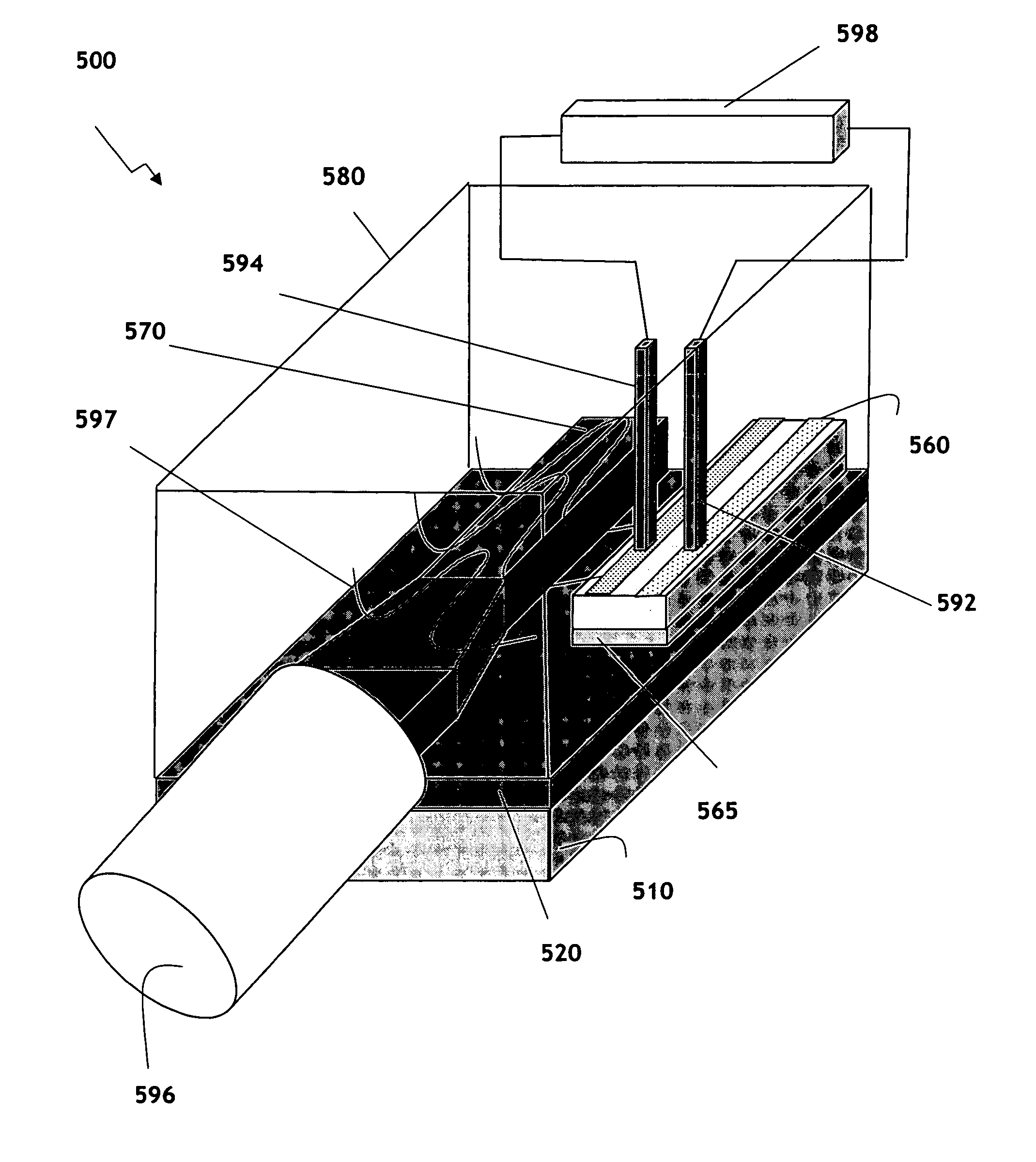
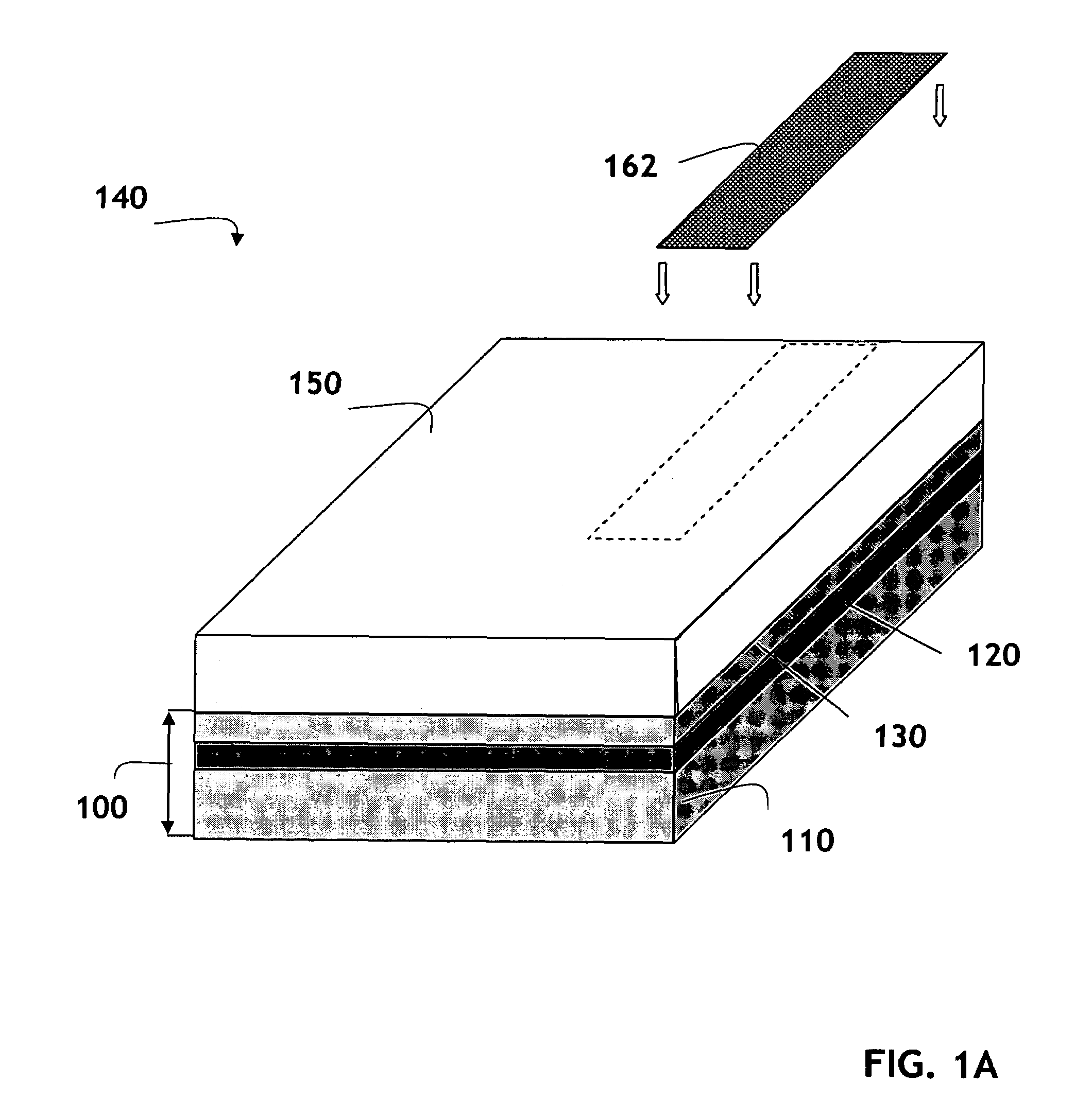
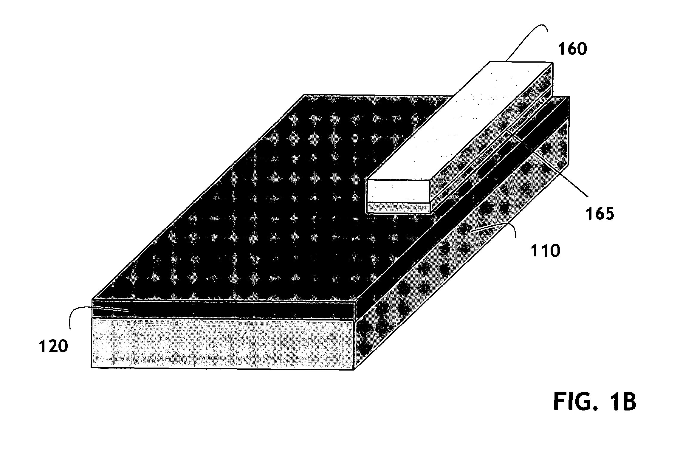
[0028]In accordance with its various embodiments, the invention disclosed herein contemplates fabrication of integrated waveguide-based photodetector apparatus with improved detection capabilities and integration density utilizing methods that are generally compatible with CMOS processing techniques. Also contemplated are optoelectronic circuits including at least one integrated photodetector apparatus, a light source for directing a lightwave thereto, and one or more electronic devices for receiving and processing an electrical signal generated in the photodetector apparatus.

[0029]As discussed in more detail below, efficient evanescent coupling between components in the integrated apparatus of the invention is facilitated by epitaxially growing a photodetector in lateral alignment with an optical waveguide, as well as by matching propagation constants of the photodetector and the waveguide. Selective epitaxy is suitable for fabricating optoelectronic devices according to many embod...


PUM

PropertyMeasurementUnit
widthaaaaaaaaaa
thicknessaaaaaaaaaa
thicknessaaaaaaaaaa

Abstract

High-speed optoelectronic devices having a waveguide densely integrated with and efficiently coupled to a photodetector are fabricated utilizing methods generally compatible with CMOS processing techniques. In various implementations, the waveguide consists essentially of single-crystal silicon and the photodetector contains, or consists essentially of, epitaxially grown germanium or a silicon-germanium alloy having a germanium concentration exceeding about 90%.

Description

FIELD OF THE INVENTION[0001]This invention relates generally to optoelectronic devices and, specifically, to methods and materials for fabrication of waveguide-based photodetector devices.BACKGROUND OF THE INVENTION[0002]Various optoelectronic applications, such as optical telecommunications and intra-chip interconnects, involve transmitting optical signals and converting them to electrical signals at high data rates. Systems for performing such transmission and conversion usually require photodetector devices compatible with the speed and bandwidth of the optical signal. Typically, these devices are PIN detectors—i.e. semiconductor devices including an intrinsic region sandwiched between a p-type region and an n-type region—that have frequency responses in the GHz range and utilize optical waveguides as a conduit for directing light to the intrinsic region of the photodetector.[0003]Generally, an optical waveguide is a planar, rectangular, or cylindrical structure having a high-ind...

Claims


Application Information

Patent Timeline
Patent Type & Authority Patents(United States)
IPC IPC(8): G02B6/12
CPCG02B6/12004G02B6/1228H01L31/022408H01L31/028H01L31/0312H01L31/105H01L31/125G02B6/305Y02E10/547
Inventor AHN, DONGHWANLIU, JIFENGMICHEL, JURGENKIMERLING, LIONEL C.
Owner MASSACHUSETTS INST OF TECH
Why Eureka
Try Eureka